Diode capacitance effect and equivalent circuit and switching characteristics
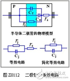
The diode has a capacitive effect. Its capacitance includes barrier capacitance CB and diffusion capacitance CD. 1. Barrier capacitance CB (Cr) As mentioned earlier, there is a lack of conductive carriers in the PN junction, and its conductivity is very low, which is equivalent to the dielectric; while the P and N regions on both sides of the PN junction have high conductivity, which is equivalent to the metal conductor. From this structure, the PN junction is equivalent to a capacitor. In fact, when a forward voltage is applied across the PN junction, the PN junction becomes narrower and the amount of space charge in the junction decreases, which is equivalent to a capacitor "discharge". The amount of medium space charge increases, which is equivalent to "charging" the capacitor. This phenomenon can be simulated with a capacitor, called barrier capacitance. The difference between barrier capacitance and ordinary capacitance is that its capacitance is not constant, but is related to the applied voltage. When the applied reverse voltage increases, the barrier capacitance decreases; when the reverse voltage decreases, the barrier capacitance increases. Varactor diodes, which are widely used at present, are made by using the characteristics of PN junction capacitance changing with applied voltage. 2. Diffusion capacitance CD When the PN junction is forward biased, electrons in the N region diffuse to the P region, forming a certain concentration distribution of non-equilibrium carriers in the P region, that is, the concentration near the PN junction is high and the concentration away from the PN junction is low. Obviously, electrons are accumulated in the P area, that is, a certain amount of negative charge is stored; similarly, holes are also accumulated in the N area, that is, a certain amount of positive charge is stored. When the forward voltage is increased, the diffusion is enhanced. At this time, the number of electrons diffused from the N region to the P region and the number of holes diffused from the P region to the N region will increase, resulting in the formation of charge accumulation in the two regions, which is equivalent For the charging of capacitors. On the contrary, when the forward voltage is reduced, the diffusion is weakened, that is, the number of electrons diffused from the N region to the P region and the number of holes diffused from the P region to the N region are reduced, resulting in a decrease in charge in the two regions, which is equivalent to The capacitor is discharged. Therefore, a capacitor can be used to simulate, called diffusion capacitance. In short, the diode exhibits two kinds of capacitance, and its total capacitance Cj is equivalent to the parallel connection of the two, that is, Cj = CB + CD. When the diode is forward biased, the diffusion capacitance is much larger than the barrier capacitance Cj≈CD; while when it is reverse biased, the diffusion capacitance can be ignored, and the barrier capacitance plays a major role, Cj≈CB. The diode is a nonlinear device, and the analysis and calculation of the nonlinear circuit is relatively complicated. In order to simplify the analysis of the circuit, a circuit composed of linear components can be used to simulate the diode. Make the voltage and circuit relationship of the linear circuit approximately the same as the external characteristics of the diode, then this linear circuit is called the equivalent circuit of the diode. Obviously the equivalent circuit is an approximation under certain conditions. When a diode is used in a DC circuit, an ideal diode model is often used for equivalence, and it can be regarded as an ideal switch. When the bias is positive, it is equivalent to "ON", the resistance is zero, and the voltage drop is zero; when it is reverse, it is equivalent to "OFF", the resistance is infinite, and the current is zero. Since the ideal diode model highlights the most basic characteristic of the diode-unidirectional conductivity, it is widely used in DC circuits and switching circuits. If considering the influence of the resistance of the diode and the threshold voltage in the DC circuit. The actual diode can be equivalent with the circuit shown in Figure Z0112. Adding a DC bias voltage across the diode and working on a small AC signal can be equivalent with a simplified circuit. In the figure, rs is the body resistance of the diode P and N regions. When the diode is forward biased, it is turned on, which is equivalent to the switch on; when it is reverse biased, it is equivalent to the switch off, indicating that the diode has switching characteristics. However, for an ideal switch, the resistance of the switch itself is zero when the switch is on, the voltage drop is zero, and the resistance is infinite when the switch is off, the current is zero, and the above characteristics are still required at high-speed switching, without switching time. But the actual diode is not ideal as a switch. Because the forward resistance and the forward voltage drop of the diode are not zero; when the diode is reversed, the reverse resistance is not infinite and the reverse current is not zero. And it takes some time for the diode to switch on and off. This limits its switching speed. Therefore, when switching, a switching diode with a small forward resistance RF, a large reverse resistance RR, and a small switching time should be selected. Gear Sensor has been widely used in the automotive and industrial field, which is important to the measurement of velocity, angel, angular velocity, direction of rotation. Gear Sensor,Custom Gear Sensor,Gear Sensor 3 Pins,Good Gear Sensor Yuheng Optics Co., Ltd.(Changchun) , https://www.yhencoder.com