Design and parameter selection method of low noise and weak optical signal amplifying circuit
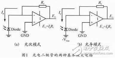
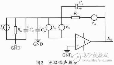
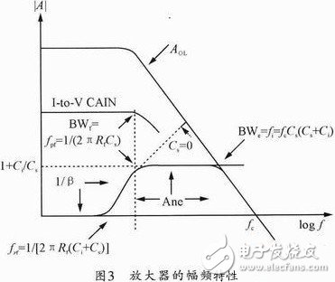
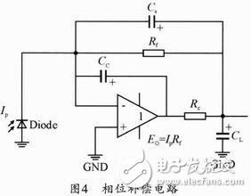
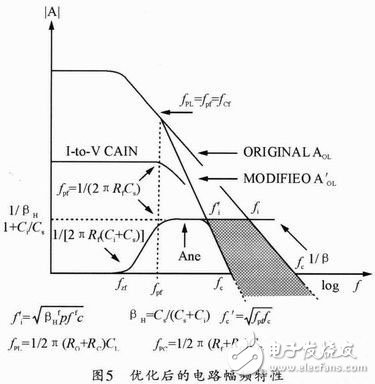
For various weak measurements, such as weak light, weak magnetic, weak sound, small displacement, small capacitance, micro flow, micro pressure, micro vibration and micro temperature difference, etc., they are generally converted into micro current through corresponding sensors. Or low voltage, and then amplified by the amplifier its amplitude to reflect the measured size. However, since the measured signal is very weak, the noise floor of the sensor, the inherent noise of the amplifier circuit and the measuring instrument, and the external interference are often much larger than the amplitude of the useful signal. At the same time, the process of amplifying the signal under test is also amplified. Noise, and inevitably add some additional noise, such as the internal noise of the amplifier and the influence of external interference, therefore, the useful signal can be extracted only by increasing the amplitude of the weak signal under the condition of effectively suppressing the noise. In this paper, the circuit noise, signal bandwidth and circuit stability of the photodiode amplifier circuit for detecting weak optical signals are analyzed. Based on this, a low noise photoelectric signal amplifying circuit is designed and the circuit parameter selection method is given. Photodiodes as photodetectors have two application modes as shown in Figure 1. (1) Photovoltaic mode, as shown in Figure 1 (a). At this time, the photodiode is in a zero-bias state, there is no dark current, low noise, and good linearity, so it is suitable for the precision field. This paper takes this mode as an example for analysis. In practical applications, this circuit generally needs to connect a small capacitor Cs in parallel with Rf to make the circuit stable. (2) Light guide mode, as shown in Figure 1 (b). This mode requires a reverse bias voltage applied to the photodiode, so there is a dark current that produces a noise current, and because of its non-linearity, it is generally used in high-speed applications. When light strikes the photodiode, the photodiode produces a weak current Ip proportional to the illumination, which flows through a feedback resistor Rf across the negative input and output of the amplifier, treating the op amp as an ideal amplifier, ideally The "dummy" characteristic at the input of the op amp, so that E0 = IpRf. It can be seen that the photodiode amplification circuit is actually an I/V conversion circuit. This circuit looks very simple and requires only a feedback resistor, a photodiode and an amplifier. The linear expression from the output voltage is easily pushed out, causing the feedback resistor Rf to increase, which will also increase the output voltage proportionally. When analyzed before, it is generally given a typical value of 100 MΩ. In the analysis below we will see that the feedback resistor affects not only the bandwidth of the signal but also the noise of the entire circuit. As a photodiode amplifier, the I/V converter has a very complex noise performance. The basic noise components are derived from the feedback resistor, the input noise current of the amplifier, and the input noise voltage of the amplifier. The noise model is shown in Figure 2. among them: CD is the photodiode junction capacitance, and RD is the photodiode id tube junction resistance. Cia is the input differential mode capacitor and input common mode capacitor of the amplifier. Cs is a feedback capacitor that eliminates oscillation and is typically 0.5 pF. Ini is the input noise current source of the amplifier, eni is the input noise voltage source of the amplifier, and enR is the thermal noise source generated by the feedback resistor. Thermal noise generated by the resistor , K=13.8×10⁻¹⁹J/°K, T is the Kelvin temperature, K is the Boltzmann constant, and the offset noise produced by the bias current is , q is the electron point charge q=1.6×10⁻¹⁹C, and IB- is the bias current. The above two kinds of noise are not affected by the operating frequency of the amplifier. The noise voltage enoe generated by the noise source eni is affected by the operating frequency of the amplifier, and the amplitude-frequency characteristics of the gain and signal gain are shown in Fig. 3. The amplification factor of the noise voltage at the DC segment and the lower frequency is 1+Rf/RD, since Rf "1, therefore this phase is approximately equal to 1 at the beginning, as the frequency increases (the corner frequency is fzf = 1 / [2πRf ( Ci+cs)], the noise gain curve first starts to rise due to the action of CD until it stops due to the action of capacitor Cs; in the high frequency band, the noise gain is limited to 1+Ci/Cs (Ci=CD+ Cia), due to Cia It is relatively small, and generally myopia considers Ci≈CD. It can be seen that the larger the RD is, the smaller the CD is, the smaller the influence on noise is, and the addition of Cs can limit the noise gain of the high frequency band. It can also be seen from the figure that the signal bandwidth is fpf =1/(2πRfCs), it can be seen that if the resistance of Rf is too large, it will seriously affect the signal bandwidth. Therefore, when selecting Rf, consider the closed-loop gain and signal bandwidth of the circuit, and choose a reasonable resistance value. The electrical signals converted by photodiodes are usually very weak and are easily interfered by external noise. Therefore, the suppression of noise in the amplifying circuit becomes extremely important. As can be seen from Figure 3, there are two measures to reduce noise, one is to reduce the noise gain. A capacitor Cf is connected in parallel with the feedback resistor Rf so that the noise gain becomes 1+Ci/(Cs+Cf). Experimental verification, coupled with Cf did not reduce the total output noise of the circuit, but only a reduction. Another more effective way to suppress noise is to limit the noise bandwidth. There are two measures to suppress the noise bandwidth. One is to reduce the open-loop gain bandwidth of the amplifier. The ideal situation is to reduce the open-loop gain of the amplifier to the cut-off point of the signal bandwidth, but this makes the choice of amplifier very limited. The second is to reduce the noise bandwidth by decoupling phase compensation. The circuit principle is shown in Figure 4. The circuit adds an RC low-pass filter between the output of the amplifier and the output of the detector circuit to filter out the amplified noise and the noise of the amplifier itself. Capacitor Cc is used to compensate for the phase lag caused by the Rc filter circuit. The capacitor Cs is used to compensate for the phase lag caused by the photodiode junction capacitance CD and suppress the noise gain peak. Generally, Rc≈Ro, Ro is the equivalent output resistance of the amplifier, which is generally based on experience and is generally considered to be Ro≈50 Ω,. Adjusting the value of Cc removes the oscillation. The noise spectrum in this case is shown in Figure 5, and the shaded portion is the filtered noise. Increasing the value of CL will shift AOL' to the left, reducing more noise, but be careful not to affect the signal bandwidth. Through the above analysis, the design principles of the low noise photodiode amplifier circuit are summarized as follows: (1) The junction capacitance CD of the photodiode should be as small as possible, and the junction resistance RD should be as large as possible. Among them, CD has an important influence on noise. RD is generally very large, with a few hundred megaohms, so its impact on noise can be ignored. (2) The photodiode should adopt a zero-bias mode of operation, which can reduce the dark current of the photodiode and improve the detection accuracy. But at the same time, we should note that at zero bias, the CD is several times larger than the reverse bias operating state, which in turn increases circuit noise. (3) The feedback resistor Rf should be as large as possible under the premise of satisfying the signal bandwidth, which is beneficial to improve the signal-to-noise ratio. At the same time, however, it should be noted that the bias current IB- of the amplifier will generate an offset voltage on the feedback resistor, so Rf should not be too large. (4) It is generally necessary to connect a small capacitor Cs in parallel with the feedback resistor, which is usually in the range of 0 to 0.5 pF. This can reduce noise and eliminate oscillation, and can better meet the signal bandwidth. (5) In the case of meeting the signal bandwidth, try to use an op amp with a small bandwidth, which is more conducive to reducing noise. When selecting components, use low noise devices. (6) The photoelectric detection circuit must use a metal casing to shield the external electromagnetic interference, and at the same time the casing is grounded. It is necessary to prevent the power supply line on the circuit board from leaking to the feedback loop and the input terminal, causing noise or drift. The input terminal leads should be made of high-insulation wires. If necessary, the amplifier can be mounted on the insulator, strictly connected to avoid cable vibration, and the input connection line should be shortened as much as possible. The feedback resistance should not be too large to avoid interference. The wiring on the circuit board should be reasonable. If necessary, the photodiode can be used. The feedback resistor is suspended and directly connected to the op amp to reduce the leakage current and improve the sensitivity of the detection. The lead distance from the photodiode output to the amplifier should be as short as possible, and the leads should be as symmetrical as possible to ensure that the impedance is basically matched. The amplifier input and output should avoid cross wiring and prevent mutual coupling. The design of the photodiode amplifier circuit is a very tedious task. Although the circuit that realizes it looks very simple, due to the complex noise representation, the signal itself is weak, and it is difficult to design a perfect low-noise amplifier circuit. This paper gives the general principles of the circuit design, analyzes the main noise characteristics of the circuit, and finally gives the parameter expressions of the optimized circuit and components. It has been verified by experiments and achieved good results, which is suitable for the detection of weak optical signals. Dust Explosion Proof Motor,Explosion Proof Induction Ac Motor,Special Explosion-Proof Motor,Dust Explosion Protection Motors Yizheng Beide Material Co., Ltd. , https://www.beidevendor.com