Establishment of wireless data transmission network for shortwave radio
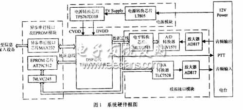
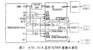
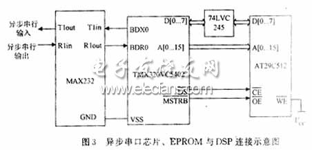
Radio shortwave refers to electromagnetic waves with a wavelength of 10 to 100 m and a frequency of 3 to 30 MHz. The use of short-wave channels for data communication has the advantages of long transmission distance, less terrain limitation, and less susceptibility to human damage. It has broad application prospects. Based on the analysis of the characteristics of short-wave channels, the article improves the short-wave radio station, the main tool of short-wave communication, and proposes a scheme for building a point-to-multipoint star topology wireless network for long-distance Data transmission, and designed the system software and hardware based on DSP chip according to this scheme. Through experimental tests, the system has realized the function of networking. 1 Network solution When designing the networking scheme, the shortwave radio station needs to be improved. In order not to affect the original internal hardware structure and function of the radio station, the scheme in this paper designs the hardware that interfaces with the audio input and output ports of the shortwave radio station. Do audio modulation, then the radio station carries on the secondary modulation to the short wave frequency band to send, after receiving the digital signal through short wave demodulation and audio frequency demodulation at the receiving end. This improved method is suitable for most radio stations with voice communication function, easy to transplant, and has good economy and versatility. Using time division multiple access (TDMA), only one user sends a signal at a time to obtain better signal-to-noise performance. The multipath delay generated in shortwave communication limits the reported symbol rate to generally less than 200 b / s. In this scheme, the symbol rate is set to 100 b / s. Multi-frequency frequency keying (MFSK) audio modulation method is selected. This method is suitable for data transmission on channels lacking phase stability and fading channels, and makes full use of the transmission bandwidth and improves the transmission rate. At the receiving end, non-coherent demodulation and square rate detection are used to demodulate the MFSK signal [1]. This method does not require the estimation of the carrier phase, which greatly reduces the complexity of the system. The sending end inserts the time domain bit synchronization pilot before sending the MFSK signal, which is used to help the receiving end obtain the bit synchronization information of the sampling decision. This scheme uses the m-sequence autocorrelation function to approximate the impulse function, and uses the m-sequence audio modulation signal with the same period as the symbol as the bit synchronization pilot. When performing pilot detection, the receiver first shifts the sampled signal sequentially and then correlates it with the local sequence. Within a symbol period, it finds the largest correlation result and the corresponding time, which is considered to be a symbol The moment of the end, and thus the bit synchronization information. 2 System hardware design 2.1 The overall structure of the system hardware The system hardware takes DSP chip as the core, mainly performs digital processing on the signal, and combines a fixed hardware structure with a flexible software algorithm. Only by modifying the software can the program improvement and system upgrade be realized, which is flexible, simple, and convenient. The system uses the DSP chip TMS320VC5402 (referred to as C5402) produced by TI. It is a 16 b word fixed-point DSP chip with low power consumption and high cost performance. Processing power has been widely used in real-time embedded voice communication and other aspects. The system hardware structure is shown in Figure 1. Mainly includes 4 modules: DSP module, power module, analog interface module and asynchronous serial interface and EPROM module. The DSP module is used to complete the digital signal processing algorithm; the power module utilizes the 12 V DC voltage provided by the radio station and undergoes two-stage power conversion to produce stable 3.3 V and 1.8 V voltage outputs, which are provided to the C5402 as ï¼ O power supply and core power supply, and the DC voltage of 5 V also supplies power to other chips on the circuit board; the analog interface module is connected to the radio audio port to sample audio output signals and generate audio analog input signals to control radio audio input and output Convert keying signal PTT; asynchronous serial interface and EPROM module complete communication with information entry equipment, save program code and load on reset. 2.2 Design of analog interface module The system hardware adopts 10 b parallel A / D converter TLV1571, the sampling rate of the chip can reach up to 1.25 MS / s, the power consumption is extremely low, and there are 2 software configurable control registers, all of which are controlled by the trigger signal Sampling, conversion and data output, simple interface and control, using a dual 8 b parallel D / A converter TLC7528, the chip is designed to have a separate on-chip data latch, settling time is 100 when VDD = 5 V ns, the transmission delay is 80 ns, and the working bit voltage mode can be used. Data latching and digital-to-analog conversion are also fully controlled by the trigger signal. Their connection with C5402 is shown in Figure 2. This module maps TLV1571 and TLC7528 to 0x0002 and 0x0001 in the I / O space through address decoding, ensuring that only one chip is in the strobe state when the C5402 accesses the data bus. At the beginning of the program, the working mode of TLV1571 must be initialized. By writing control words 0x00C0 and 0x0100, he is configured to use internal clock, software to start sampling, and binary output mode [2]. C5402 sets the serial port pin FSX0 as a general-purpose output pin to control the read signal of TLV1571. In each timed interruption, a corresponding trigger signal is generated to start D / A and A / D conversion. By changing the frequency of the timed interruption, the sampling rate and D / A conversion frequency can be flexibly changed. 2. 3 asynchronous serial interface and EPROM module design Asynchronous serial interface and the connection of EPROM module and C5402 are shown in Figure 3. This solution uses the two pins of the buffered serial port McBSP0 of the C5402: BDR0 and BDX0 as general input and output pins to simulate asynchronous serial ports. The MAX232 chip is used to convert the TTL level output by the C5402 to an electric power that complies with the RC232 standard It can communicate with devices that comply with this standard. The EPROM chip uses AT29C512, and its storage capacity is 64 k & TImes; 8 b, which is used to store program codes and complete bootstrapping.
A 16V Desk-top power supply can be battery charger for your
laptop/ CCTV Cameras, or power backup for your bluetooth speaker/stage lighting,
or external power source for your massage chair, or power station for your
electrombile. A desktop power adaptor can be used everywhere in your life. With
the over-current protection/over-load protection/over-voltage protection and
short circuit protection, our desktop power supply assured you a perfect safety
usage. At the same time, every piece of power adaptor that we produced, was get
through 100% full-load burning test for at least 2 hours, and 3000Vac
withstanding voltage test for 1 minutes. The conversion rate of our desktop
power supplies is 85%, which is much higher than other factories.
16V Desktop Switching Power Supply 16V Desktop Switching Power Supply,Desktop Switching Power Supply,Switching Power Supply Shenzhen Juyuanhai Electronic Co., Ltd. , https://www.powersupplycn.com