Design of Face Recognition System Based on DSP
For the face recognition related algorithm can run quickly, select TI's DSP processor, and add keyboard module and PAL system output module, which can separate and process PAL video signals independently from PC, and independently operate face positioning. , feature extraction and face recognition. In terms of hardware, the system adopts a memory switching system, so that image data buffering and reading are performed independently and simultaneously by CPLD and DSP, which shortens the processing period of data and ensures the real-time operation of the system. Software design includes: face positioning, human eye positioning, sample storage, and face recognition. The sample is automatically selected by the DSP, and is determined according to the size of the human eye and the size of the face marker box. A part of the image of the same size and the same eye distance is selected as the training sample and the sample to be identified. In the process of principal component analysis, the principal component is extracted to form the feature face space, and the original sample is projected into the space, and then sent to the KNN classifier for classification. The device is easy to carry, low power consumption and can be applied to other fields through software design, such as motion recognition, dynamic tracking and so on. 1 Face detection algorithm The face detection system can be divided into face detection and face recognition modules. The two modules can be further divided into four modules: face detection and localization, normalization, feature extraction and face recognition. Its detailed structure is shown in Figure 1. 1.1 Positioning of the face It is an important step to judge the position of the face by the obtained sample, select the appropriate face, and take out the sample. Face feature location and feature extraction quality have a direct impact on face image recognition. First, the coordinates (x1, y1) and (x2, y2) of the human eye are determined, thereby indirectly obtaining the coordinates of the upper left vertex and the lower right vertex of the square face, which are respectively set to (X1, Y1) and (X2, Y2). ), its detailed calculation method is as follows Where RH and RV are empirical constants, which are taken to be 2.0 and 3.5, respectively, during the design process. In this way, the area coordinates of the face can be obtained in the original picture, and the size varies with the size of the eye distance Widtheyes. However, as the input of the PCA, the dimension of the input sample is required to be the same, so the picture must be normalized. The resulting face region samples were scaled to 24 & TImes; 24 in the design. In addition, it is necessary to perform contrast adjustment and histogram equalization on the image to improve the accuracy of recognition. 1.2 Face feature extraction When designing a face recognition classifier, a picture is usually treated as a one-dimensional vector. Although this is different from the traditional way of viewing pictures as a matrix, it can create favorable conditions for feature face extraction using principal component analysis (PCA). The method of feature face classification is to project an image to a point in a specific "face space". This "face space" consists of a series of mutually orthogonal vectors. These vectors are an important part of characterizing each face cluster. The pictures of different faces are far apart in this space, and the projections of different pictures of the same face are close to each other in this space. Therefore, the PCA method can be used to lay the foundation for the entire face recognition system. In the first step, N samples are collected for use as the training set X, and the sample mean m is obtained, as shown in equation (1). Among them, xi∈ sample training set X = (x1, x2, ..., xN). In the second step, the scatter matrix S is obtained, as shown in equation (2). According to the basic principle of PCA, the eigenvalue λi of the scatter matrix and the corresponding feature vector ei must be found. Where ei is the principal component, and the size of its corresponding feature value represents how much information it contains. Therefore, it is necessary to arrange λ1, λ2, ... in order from the largest to the smallest. As shown in Fig. 2, the left side is a face image reconstructed by the eigenvector corresponding to λ1, which can basically distinguish the contour of the face, and the right side is an image reconstructed by the eigenvector corresponding to λ100, which looks more like noise if it will Its application to the system is unfavorable for identification. Suppose that p values ​​are taken, λ1, λ2, ..., λp can determine the face space E = (e1, e2, ..., eP), in this face space, in the training sample X, each element is projected to the point of the space Can be obtained by equation (3) Obtained from the above formula is the p-dimensional vector after the original vector is reduced by the PCA. The next step is to input it into the KNN classifier for classification. 1.3 Construction of KNN classifier The implementation of KNN is divided into two steps of training and recognition. During training, the results of dimensional reduction of each type of sample are used as input to KNN. The K-nearest neighbor algorithm classifies a test point x into the most prominent of the K nearest neighbors, grows from the test sample point, expands the area until it contains K training sample points, and puts the test sample The category of points is classified as the most frequently occurring category among the most recent K training sample points. As shown in FIG. 3, the circle indicates the position where the data to be identified is located. When the K value is 3, three data in the solid circle are selected, and the recognition result is a class represented by a triangle; when the K value is 5, the dotted line is selected. The five data in the circle, the recognition result is the class represented by the square. So choosing the right K value has a great impact on the classification results. If the K value is chosen too large, it may be classified more correctly, but at the same time it sacrifices performance and improves computational complexity. If the K value is chosen too small, the computational complexity is greatly reduced, but the accuracy of the classification may be affected. 2 system hardware design The DSP6713 is used in the system design. This is the C6000 series floating-point processor produced by TI. It adopts the VLIW architecture, and the equivalent cycle number of the command operation is lower and the running speed is faster. The image is captured by the ordinary camera with PAL output and the image encoding chip TVP5147 produced by TI. The chip supports multiple formats, multiple interface inputs, and can output video data in YUV format, while providing line sync signal and vertical. Synchronization signal, etc. Data staging is implemented using CPLD and SRAM. Design system composition, as shown in Figure 4. 2.1 TVP5147 chip When the system is powered on, the DSP first initializes the TVP5147, which is implemented by the I2C bus, and the DSP comes with an I2C bus controller. The chip I2C address is controlled by the level of the chip pin I2CA. If the pin is connected to a high level, the I2C write address is 0xB8, otherwise it is OxBB. The first behavior in the figure is the DATACLK signal, which is the data clock signal provided by the TVP5147 chip, and the second behavior data Y[9...0]. When each line of image starts, there will be 4 SAV signals. Similarly, there are 4 after the end. The EAV signal, as shown in FIG. 5, is in the YCbCr format, and the data of each pixel is composed of 4 data, one time being Cb, Y, Cr, Y. It can be seen from FIG. 5 that when the AVID signal is at a high level, it indicates that the current data is valid data. This provides a reference signal for the CPLD to acquire valid data. At the same time, the TVP5147 chip also outputs an FID signal, which is a parity field indication signal. If the system is initialized from Y[9. . The O] port outputs 10-bit YUV mixed video data, and it can be known that its output meets the following timing, as shown in FIG. 5. 2.2 CPLD read and write SRAM The memory selects the DS1265AB, which is an SRAM memory that has the advantage of fast memory and the ability to save data for 10 years when the system is powered down. The DS1265 has a capacity of 1 MB, 20 address lines, 8 data lines, and a WE, OE, CE signal input. CPLD's choice of EPM7128 has the advantages of low price and high counting frequency. Connect the memory SRAM to the IO pin of the CPLD, and the timing of the SRAM can be read and matched with the timing. The schematic diagram is shown in Figure 6. The CPLD program is written so that the output timing satisfies the storage requirements of the SRAM. Of course, for the specific requirements of the design, the two pieces of SRAM are used to store the data of the odd-even field respectively. The switching of the SRAM is realized by the odd-even field signal FID controlling multiple pieces of the 74HC245, the detailed process, such as Figure 7 shows. When FID is at a high level, M1 and M4 are enabled at this time. At this time, CPLD inputs address signal CPLDaddr into SRAM1, DSP inputs address signal DSPaddr into SRAM2, and M6 and M8 are enabled. As can be seen from the figure, At this time, the CPLD writes data to the SRAM1, and the DSP is reading data from the SRAM2. At the same time, the M10 is enabled, the CPLD signal CPLDctl controls the reading and writing of the SRAM1, and the DSP signal DSPctl controls the reading and writing of the SRAM2, when the FID is converted to At low level, SRAM1 and SRAM2 are just swapped. The system constructed in this way can simultaneously record two fields of video at the same time, realizing the organic combination of CPLD and DSP. At this point, the task of the CPLD is to store the valid image data in the corresponding SRAM. When the AVP pin of the TVP5147 chip rises, the address is set to the initial value of 00h, that is, the first address is sequentially written backward. Each data clock signal DATACLK rising edge stores the Y[9...2] output from TVP5147 to the current address unit, and the Y0 and Y1 bits are discarded because the selected SRAM data bit is 8 bits. When the Y0 and Y1 bits are discarded, The accuracy of the image data is reduced, but the effect on the recognition effect is small. Then, with each rising edge of DATACLK, the CPLD adds 1 to the address unit, thus realizing the writing of each field of data. When switching to another field of data, the process of execution is the same, except that the stored object is forcibly changed by the 74HC245, so that each field of data can be recorded. 2.3 Image output system design In order to reduce the burden during system design, the TV set is connected to the DSP bus through TI's video encoding chip THS8135, and the obtained YUV data is directly output to the video receiving end of the TV AV through the THS8135, and through the DSP. Some information can be displayed on the TV screen, which makes the process of identification more human. 3 system software design After the system hardware is successfully debugged, it is necessary to provide certain software algorithms, etc., in order to realize the combination of software and hardware. In this design, the SRAM is extended on the DSP processor EMIF, and the DSP processor will activate the effective parity field by the trigger of the read signal. The data is stored as two one-dimensional arrays for processing. 3.1 DSP image preprocessing The image data output by the TVP5147 chip is not in RGB format, but is output in YUV format. The image processor needs to be converted into RGB format by the DSP processor, and the conversion formula is as shown in equation (4). The DSP reads the image data into the memory space, and then operates on it, and puts the obtained RGB into the corresponding storage unit, and calculates the gray value Gray, and the operation formula is as shown in the formula (5). The resulting gray value is stored in the corresponding array. Each picture consists of two pictures, so the full picture resolution is 720×576. But for the system itself, there is no need to convert every pixel, so the 320×240 is intercepted for storage, so the resolution of each field is 320×120, which greatly reduces the pre-processing and face positioning from YUV to gray image. Time has improved the performance of the system. 3.2 Face Discrimination Process After the obtained 320×240 picture is detected by the face, the part of the face is taken as a face sample. At the time of design, all samples of the face will be displayed on the display, which reduces the possibility of face error detection and improves the accuracy of the system to some extent. The sample resolution of the face is 24×24, which is input to the PCA as a one-dimensional vector of 576 dimensions. Figure 8 (a) is a flow chart for calculating the PCA projection matrix, and Figure 8 (b) is a working flow chart of the KNN classifier, wherein the value of the training sample after PCA projection does not need to be recalculated in each recognition, and can be used as The calculation at the time of initialization can also be stored in the power-down non-volatile medium, such as the flash memory, which can improve the operating efficiency of the device and reduce the amount of calculation. As shown in Figure 8, the KNN classifier can determine the closest classification, but does not reject the classification, so that any person's face will be assigned to a class of built-in sample sets. Such a classification method is not advisable, so it is necessary to add a decision as to whether or not to reject, and the flowchart is as shown in FIG. As shown in the flow chart, when the sample points are reduced by the PCA and then sent to the KNN classifier for classification, the obtained result must be judged as the Kth class. At this time, the conclusion cannot be made, and the point to be measured and the K class are first obtained. The sum of the Euclidean distances of the sample points of the label. Define two thresholds a and b, if sum 4 test results In this experiment, the value of a is selected to be 12 400 and the value of b is 16 200. The determination of these two values ​​requires a large number of experiments to find out the law. The value of x directly affects the effect of recognition. The paper selects x=4 and x=5 for testing. (1) When x=4: When testing the 36 face images of 12 people in the identifiable library, the program correctly recognizes 33 of them, and the other 3 images are judged as no, 0 judgment errors. When the program tests 33 face images of 3 people in the unrecognizable library, 22 images were successfully rejected, and 11 images were misjudged; (2) When x=5: When testing the 36 face images of 12 people belonging to the identifiable library, the program correctly recognizes 25 of them, and the remaining ll images are judged whether or not. When the program tested 33 face images of 3 people in the unrecognizable library, 28 images were successfully rejected and 5 were misjudged. Analysis of the above experimental data shows that when x=4, the recognition rate of the identifiable library is 91.6%, and the rejection rate of the unrecognized library is 66.7%. When x=5, the recognition rate of the identifiable library is 69.4-%, and the judgment rate of the unrecognized library is 84.8%. Therefore, when applied to different occasions, different x values ​​should be selected. When it is required to reject foreign faces as much as possible, the optional x value is 5. When it is required to identify known faces as much as possible, the optional x value is 4. 5 Conclusion The construction of this face recognition system fully considers its popularization. Instead of using a USB camera as an image acquisition device, the analog camera of the universal video standard is replaced, so the user can be more free when the camera is selected. At the same time, the device supports a variety of interface inputs, in addition to the ordinary R-jack port, it also provides input methods such as Svideo, YPbPr and RGB. The recognition accuracy of the device can reach more than 90%, which basically meets the identification requirements. The system has good real-time performance and is easy to carry. It can be extended to dynamic image tracking and motion detection through program modification.
12mm Key Switches including Electric Key Switch, Key Lock Switch, CAM Lock , belongs to power lock. It can save space and easily operate with the "innovation and convenience" design concept. The whole series products are widely used in human-machine panel so it can greatly reduces the space of the control panel. Meanwhile,its shape is different from the other switches,for example Metal Switches , Automotive Switches, Push Button Switches.
Production control of 12mm On Off Key Switch: In order to provide competitive price, quality and stable delivery cycle of the whole series of 12mm power lock switches, the company has the world's advanced CNC production machine and a number of fully automated processing equipment and has successfully imported Toyota lean production system.
It all adopt the One-stop operation and automated production assembly from development and design,mold manufacturing, zinc-aluminum alloy die-casting, plastic injection, stamping, lathe polishing, baking varnish, product assembly, to quality assurance inspection, etc. As a result, we have accept Japan, Europe and the United States hardware construction industry, as well as large European and American companies commissioned to undertake the manufacture of various locks and related hardware parts.
Diversification of 12MM power lock products: The whole series of power lock products have complete functions. In order to improve the safety and confidentiality of customers' using experience, we could offer customers with different keys to achieve the effect that the keys cannot open each other.
12MM Key Switches 12Mm Key Switches,Electric Key Switch,12Mm Key Lock Switch,12Mm On Off Key Switch YESWITCH ELECTRONICS CO., LTD. , https://www.yeswitches.com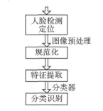
Figure 1 Face recognition algorithm flow 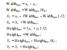


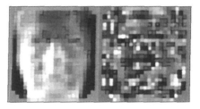
Figure 2 reconstructing the face image 
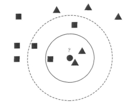
Figure 3 KNN classifier 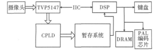
Figure 4 system structure block diagram 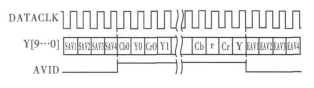
Figure 5 TVP5147 output timing 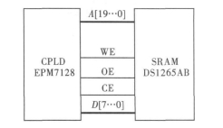
Figure 6 Schematic diagram of CPLD and SRAM connection 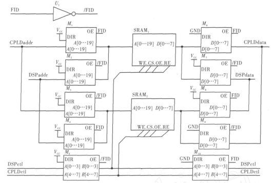
Figure 7 SRAM switching circuit diagram 

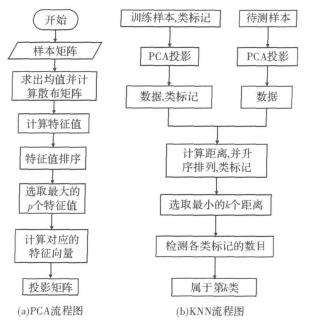
Figure 8 PCA and KNN flow chart 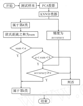
Figure 9 Human face classification flow chart
