Design of multi-protocol programmable interface based on digital chip
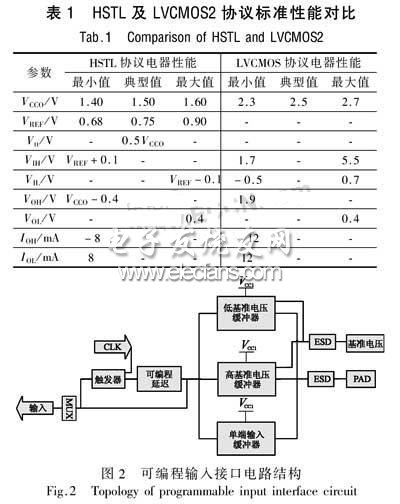
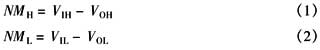
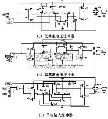
introduction With the continuous development of process technology, high-speed memory and multiple bus standards are more and more widely used in high-performance digital chips, and it is necessary to provide reference voltages with multiple level standards, which poses challenges to the design of interface circuits. It is urgent to design a programmable input and output interface circuit that supports high-speed communication, high-coverage level standards, supports multiple interface protocols, controllable delay, and has a certain working speed, stability, and high driving capability. Based on the above analysis, this paper designs an input interface circuit in a multi-protocol programmable input and output interface. In the case of the user configuring the reference voltage and input mode, it can support up to 10 different protocol standards, and can be programmable The delay module eliminates the holding time from the pad to the chip to achieve synchronization of the signal path. 1 Circuit topology and protocol analysis At present, the input-output interface module (IOB) of the high-performance digital chip usually adopts the topology structure shown in FIG. 1, which completely provides the connection from the pin to the internal logic of the chip. The structure is mainly composed of programmable input buffer, programmable output buffer, input trigger latch, output trigger, programmable delay and ESD protection. Each IOB controls a pin, which can be configured as input, output or bidirectional I / O function. When the pin controlled by the IOB is defined as an input, the input signal through this pin is first sent to the programmable input buffer. The output of the buffer is divided into two channels: one channel can be directly sent to the multiplexer and input to the chip after selection; the other channel is delayed by a few nanoseconds (or directly input without delay) through the programmable delay module, and then sent to The input path trigger is sent to the data selector. The data selector is controlled by programming, and the input and output flip-flops are equipped with independent clocks. The rising or falling edge can be optionally used as the effective action edge to achieve programmable control of the input and provide different interface protocols. JEDEC defines the electrical performance of the input and output interfaces, including the supply voltage, the lowest input high level VIH, the highest output low level VIL, the lowest output high level VOH, the highest output low level VOL, the maximum current drive capability, the output slew rate In addition, it is necessary to provide a user-defined reference voltage VREF for differential input according to a specific input and output standard. Taking the higher frequency HSTL standard and the more general LVCMOS protocol standard as examples, the electrical performance defined by JEDEC is shown in Table 1. It can be seen that different input buffer modules must be designed to provide input paths for different standards. The swing voltage of the HSTL protocol is low, the frequency can reach 200 MHz, but it does not have the 5 V voltage withstand capability, and it must be differentially input. It is necessary to provide a 0.75 V reference voltage from the outside; the LVCMOS protocol has a high voltage and strong withstand voltage. Single-ended input, single-ended end-to-end input buffer is optional. According to the 9 different protocol characteristics in Table 1, it is divided into three groups, input through different input buffer modules, respectively programmed and controlled, and the amount of delay is added as needed. The circuit structure of the module is shown in Figure 2, where the programming control points are not given. Among them, the low reference voltage buffer completes the protocol differential input of the lower reference voltage, including the HSTL / GTL / GTL + protocol, the reference voltages are 0.75, 0.8, and 1.0 V, respectively; the high reference voltage buffer completes the protocol differential input of the higher reference voltage , Including CTT / SSTL2 / SSTL3 agreement, the reference voltage is 1.5, 1.25, 1.5 V respectively; The single-end input buffer finishes the end-to-end general agreement input, including LVTTL / LVCMOS / LVCMOS18 agreement. The programmable delay module performs programmable delay on the signal of the signal input path to synchronize it with the clock signal CLK of the D flip-flop, and finally selects the signal as a direct input or a delayed input through a selector (MUX). 2 Circuit realization For low reference voltage buffers, the design uses PMOS differential input stages. The key factors that affect the performance index include the gain of the input differential amplifier, noise tolerance, and common-mode rejection capability. The highest frequency in the input protocol is the HSTL protocol, which can reach operating frequencies above 200 MHz. Taking the HSTL protocol as an example, the JEDEC8 standard defines two logic standards, DC and AC, and there is a level difference of approximately 100 mV between the two standards. This is because when the input signal is always greater than the DC threshold, the logic state can be kept stable, avoiding flipping, which facilitates the design of high-gain differential input stages. Noise tolerance NM is a particularly important indicator in input and output circuits. Too low a noise tolerance can easily cause logic errors. High noise tolerance NMH and low noise tolerance NML are defined as For the HSTL protocol, the typical VMH and NML for single-ended input are both 250 mV, and the differential input can suppress 650 mV of common mode noise. In design, the equivalent small signal gain gm of the differential input tube should be increased as much as possible. , Improve the common mode rejection ratio CMRR. To prevent substrate noise from coupling into the input path, you can add a guard ring to the layout to isolate it. The design idea of ​​the high-reference voltage buffer is basically the same as that of the low-reference voltage buffer, but the input terminal uses an NMOS differential input stage. The basic structure of a single-ended input buffer is similar to a Schmitt trigger, with a higher input threshold voltage. After the input signal reaches the threshold voltage, the output is flipped through the buffer and shaped. The programmable delay module adopts a multi-stage inverter delay line structure, and has multiple selection input paths. The difference in the number and size of inverters in each path is used to control the amount of delay through four switch tubes. Before entering the chip, the delayed signal and the non-delayed signal can also be selected by a multiplexer MUX to meet the different needs of the internal clock. The final circuit is shown in Figure 3.
The quality is the life of the product. The finest quality are always our pursuit. We special emphasis on the quality of the product. No matter how many quantity or urgent delivery of orders, every order will be good take care of for us. Prompt delivery and competitive price are also our advantages which have earned the trust and respect from our customers. We specialized in the production of LED lights, our products are sold to different countries and regions all over the world.Such as led tube light,g24 led tube light.
G24 Tubes,18W G24 Tubes,13W G24 Tubes,9W Led Tube G24 SHENZHEN KEHEI LIGHTING TECHNOLOGY CO.LTD , https://www.keheiled.com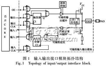
The focus of this work is to design the programmable input sub-module circuit in this module, which mainly includes programmable delay module, programmable input buffer module, ESD protection module, input trigger latch, selector, etc. The design goal is to complete multiple Programmable selection of universal and high-speed input standard protocols. The current highly integrated interface protocol is called the JEDEC (joint electron device engineering council) standard. Common input and output interface standards are defined in the JEDEC8 series.