SoC FPGA: Adaptive Performance Analysis in Product Development
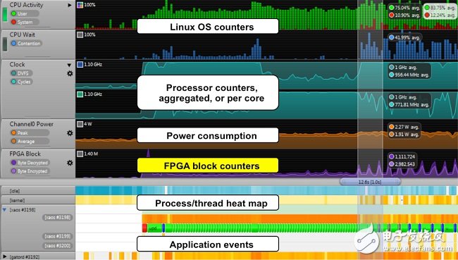
The purpose of the development tools is not only to debug complex problems, but also to improve development efficiency. Sometimes, the achievement of this goal depends more on the convenience and utility of standard product characteristics than effective power characteristics. A great convenience feature in most professional debuggers is the register bank to display the memory mapped SoC peripheral registers, including their names, bit fields, and descriptions, which are consistent with those in the peripheral documentation. When developing for an FPGA, it is more complicated. FPGA vendors typically provide FPGA hardware libraries such as encryption/decryption modules, math algorithm acceleration modules, and peripheral controllers. However, hardware developers are required to determine how many modules are integrated into the FPGA to determine where in the memory they are located in the memory map, which means that the software debugger cannot provide a peripheral register view immediately. Software developers can manually generate debugger peripheral description views, but manual editing is time consuming and error prone. The solution requires communication between the FPGA synthesis tool and the software debugger. The Altera QSys System Configuration Tool generates peripheral register description files for a complete FPGA design. The ARM DS-5 Debugger automatically imports files and displays FPGA IP registers as if they were part of a hard processor system. Figure 1: Automated generation of peripheral register views and import on the DS-5 debugger System level performance analysis Today, product developers are more concerned with debugging performance issues, trying to implement more features on the same hardware, or reducing power consumption. As a result, tool vendors are increasingly focusing on performance and power analysis tools. One of the main reasons for choosing SoC devices (with integrated processor and FPGA architecture) is the ability to use FPGA hardware blocks to speed up software work. For example, the FFT decoder or the DES decryption algorithm in the FPGA fabric can be used to free the processor, allowing the processor to perform other tasks, or to go to sleep to save power. For these devices, the tool should be able to view the relative level of processor and FPGA IP module resource usage. Designers can then use this information to optimize the system. Although instruction tracking is used to optimize software codecs and other performance software, for ARM application processors running Linux and Android operating systems, some specific analysis, such as the ARM DS-5 Streamline Performance Analyzer, is required. tool. The ARM DS-5 uses the Linux driver running in the target to sample the information at regular intervals, each time the event counter provides captured task switching information, such as: ◠Operating system events such as processor load. ◠Processor events such as branch mispredictions. ◠System events that allow users to find system level bottlenecks. ◠Software notes for reporting events of interest. After seeing this information appear on a timeline, developers understand the interaction between software and hardware. For hybrid processors and FPGA devices, streamline analyzers can be used to optimize both hardware and software. The only basic component required in hardware is the memory-mapped registers, which calculate the utilization of each different IP block. Streamlines can then be configured to access these new counters, display their values ​​over time, and correlate with CPU usage and other system-level counters. Figure 2: Timeline view in the ARM DS-5 streamline. Users with power requirements can extend the streamline with ARM energy probes to monitor and view the voltage and current consumption on certain power paths in the target. On the FPGA target, these power lines typically power the CPU subsystem, FPGA core, and FPGA I/O, but they also monitor the main power supply for the entire product. By looking at the relationship between power consumption, software activity, and system utilization, as well as being able to benchmark energy consumption, developers can optimize the system for power consumption and battery life. in conclusion SoC's new devices, including ARM application processors and FPGA architectures, offer new opportunities for more efficient products. Innovations in on-chip debug hardware, FPGA tools and software debugging, and analysis tools have been matched to hardware innovations, so developing these devices and leveraging their power characteristics has become as simple and efficient as developing software on fixed ASIC devices. Digital currency transactions allow users to convert existing digital currencies into other digital currencies. The entire transaction does not involve any legal tender. Because of the relatively loose regulation, the mainstream digital currency trading platform also opened this function.Digital Asset Exchange (DAE) is a platform for matching transactions between digital currencies, digital currencies and legal currencies. It is the main place for encrypting the circulation and price determination of digital currency transactions. Currency Exchange,Digital Currency Exchange,Virtual Digital Currency Exchange,Display Currency Exchange China youbi digital assets limited , https://www.ubcoinchina.com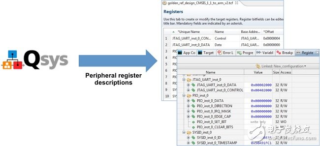
Compared with traditional stock exchanges, digital asset trading platform not only matches transactions, but also plays the role of market maker and investment bank. The role of the market maker in the trading platform can increase the liquidity of the market, and the trading platform can earn the transaction price difference. The role of the investment bank of the trading platform is to provide services such as issuance and underwriting of digital currency, from which the trading platform collects money fees, or collects deposits in the form of community voting of the trading platform.