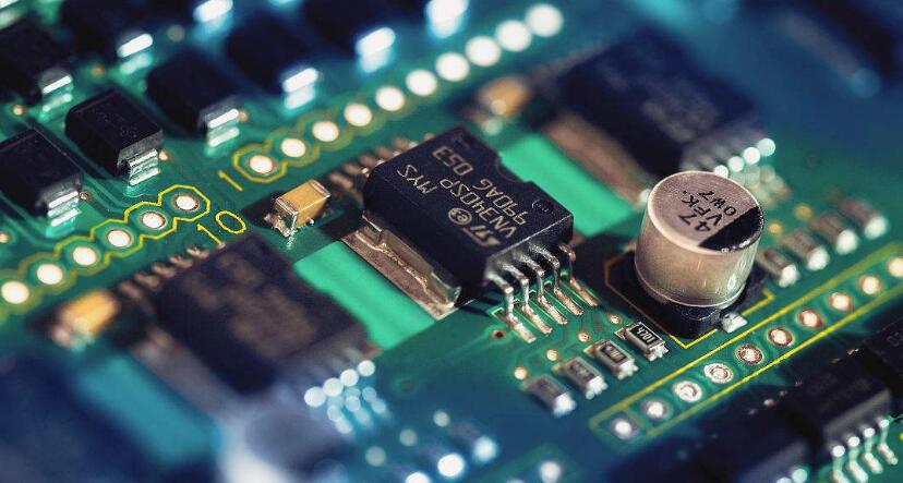
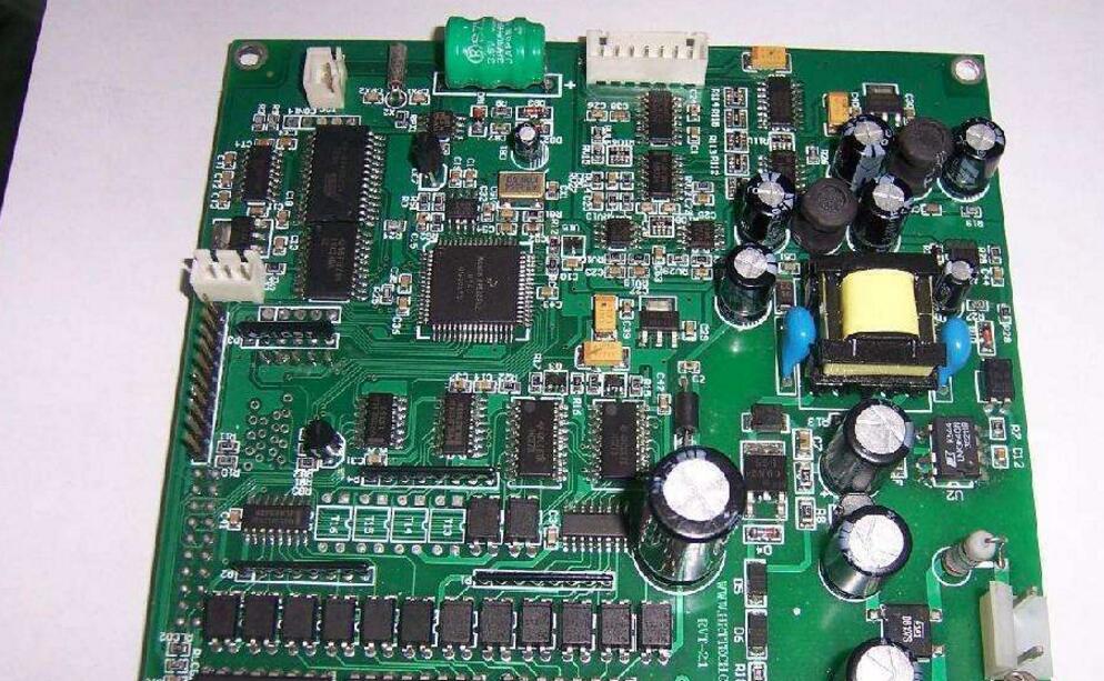
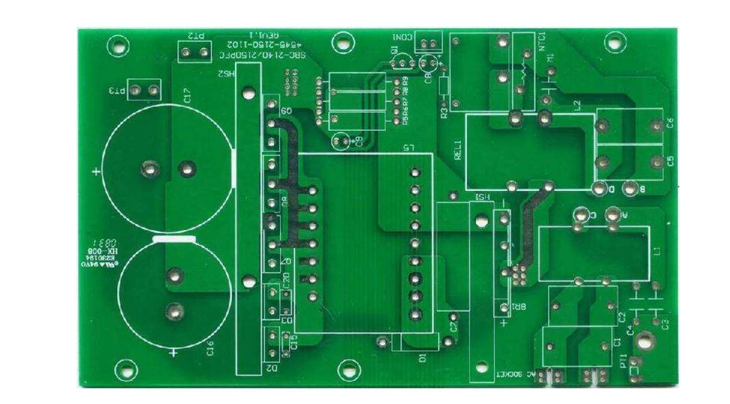
Double-sided circuit board how to see how the difference between the positive and negative circuit board
Double-sided tin plate / gold plate production process: Cutting ------Drilling -----Sinking copper ----Line --- Electrode ---Etching --- Solder resistance --- Character --- Spray tin ( Or Immersion Gold) - Edge-v-cut (some boards do not need) ----- flying test - vacuum packaging Double-sided gold plate production process: Cutting ------Drilling -----Sinking copper ----Line --- Electricity --- Plating --- Etching --- Solder resist --- Characters --- --- Edge side --- v cutting --- flying test --- vacuum packaging Multi-layer tin plate / gold plate production process: Cutting ------Inner layer-----Laminating ----Drilling---Sinking copper ----Line --- Electrode ---Etching --- Resistance welding ---Character--Spray Tin (or Immersion Gold)-edge edge-v-cut (some boards do not need)--flying test----vacuum packaging Multilayer gold plate production process: Opening ------Inner layer-----Laminate ----Drilling ---Sinking ----Line ---Chargering ---Gold Plating --- Etching --- - Solder resistance - Characters - Edge - - - - v - - flight test - vacuum packaging 1, graphic plating process Foil Plates--"Unloading--"Drilling Reference Holes--"CNC Drilling--"Test--"Deburr--"Electrolessly Plating Thin Copper--"Plating Copper--"Test--" Brush Plate--"Film (or Screen Printing)--"Exposure Development (or Curing)--"Test Fix Plate--"Graphic Plating (Cn Ten Sn/Pb)--"Defilming--"Etching--" Inspection Repair Plate--"Plug Nickel Plating--" Hot Melt Cleaning--"Electrical On-off Inspection--"Cleaning Process--"Screen Printing Solder Resist Pattern--"Curing--"Screen Printing Symbol--" Curing --" shape processing - "cleaning and drying -" test - "packaging -" finished product. Process of electroless plating Thin copper - "electroplated thin copper" these two processes can be used "chemical plating thick copper" an alternative process, both have their own advantages and disadvantages.Pattern plating - etching method of two-faced metallization is typical of the sixties and seventies In the mid-1980s, the bare copper-clad resistance film process (SMOBC) gradually developed, and it has become a mainstream process especially in the manufacture of precision double-sided panels. 2. SMOBC process The main advantage of the SMOBC board is that it solves the solder bridging short-circuit phenomenon between the thin lines. At the same time, due to the constant lead-tin ratio, it has better solderability and storage than the hot-melt board. There are many methods for manufacturing SMOBC boards. There are SMOBC processes that subtract the lead and tin from the standard pattern plating. The SMOBC process is replaced by tinning or immersion tin instead of the subtractive plating pattern of lead and tin; the SMOBC process is plugging or masking. Addition method SMOBC process. The following mainly introduces the SMOBC process and the SMOBC process of plugging the lead and tin in the pattern plating method. The SMOBC process of retreating lead-tin from the pattern plating process is similar to the pattern plating process. Only changes after etching. Double-sided Copper Clad Laminate--"Pattern Plating Process to Etch Process --" Lead-Lead Tin--"Check--"Cleaning--"Resistance Solder Pattern--"Plug Nickel Plating--"Plug Plugging Tape --" Hot air leveling - "Cleaning -" screen printing mark symbol - "" shape processing - "cleaning and drying -" finished product inspection - "packaging -" finished product. 3. The main process flow of plugging method is as follows: Double-sided foil--"Drilling--"Electroless copper plating--"Electrical plate copper plating--"Plug hole--"Screen printing image (just like)--"Etching--"to screen printing material, To plug the hole material - "cleaning -" solder resist pattern - "plug nickel, gold-plated -" plug stickers tape - "hot air leveling -" The following process and the same to the finished product. The process steps of this process are simpler and the key is to block the pores and wash the pore blocking ink. In the hole blocking process, if a hole blocking ink blocking hole and screen printing image are not used, a special masking type dry film is used to mask the hole and then exposed to form a positive image. This is the masking hole process. Compared with the plugging method, it does not have the problem of cleaning the ink in the hole, but it has a higher requirement for masking the dry film. The basis of the SMOBC process is to make bare copper metallization double-sided panels first and then apply the hot-air leveling process. The so-called single-sided and double-sided surfaces have different layers of copper. Both sides of the board have copper on both sides of the board, which can be connected by vias. On the other hand, there is only one layer of copper on one side, and only simple lines can be made. The holes made can only be used for plug-in. Single-sided board On the most basic PCB, parts are concentrated on one side and wires are on the other side. Because the wires only appear on one side, this kind of PCB is called Single-sided. Because single-board has many strict restrictions on the design circuit (because there is only one side, the wiring can not cross and must be routed alone), only the earlier circuit uses this kind of board. Both sides of the double-sided board have wiring, but to use both sides of the wire, proper circuit connections must be made between the two sides. This "bridge" between circuits is called a via. The via hole is on the PCB, filled with or coated with a metal hole, and it can be connected to the wires on both sides. Because the area of ​​the dual panel is double that of the single panel, the dual panel solves the difficulty of wiring in the single panel (via the vias to the other side), which is more suitable for use in more complex circuits than a single panel. The double-sided printed circuit board has two upper and lower conductor patterns, and the upper and lower via holes are communicated by expensive perforations. In the processing of printed circuit boards, the perforated hole walls are plated with a copper layer to make the upper and lower layers conductive. The double-sided printed circuit board is usually a double-sided copper-clad laminate, using screen printing or photoimaging. A resist pattern is formed on the copper surface, and excess copper foil is chemically etched to form a conductor pattern. There are many small points on the circuit board that are reversed, that is, the side with tin behind. Many friends are asking whether a PCB is positive or negative. Here we must pay attention to, if a PCB file only line, other characters are not there? On the first side, we must confirm whether this line is painted on the top floor or on the lower floor. If it is on the top floor, then it is logical that he is positive; if it is the lower floor, it is the opposite. However, this argument is logically inferred. Some are counter-intuitive, so it's best to ask the customer. If it is a double panel there is no such problem. If the PCB file has more characters on it, it will be better differentiated. If the character is correct, then the layer is positive. If it is negative, it is the opposite. It is such a distinction. Home Audio Speaker,10 Woofer Speaker,10 Inch Woofer Speaker,Portable Woofer Speaker Guangzhou Yuehang Audio Technology Co., Ltd , https://www.yhspeakers.com