Reading a double-sided circuit board welding method
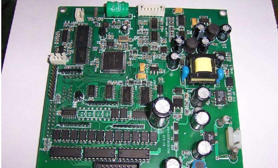
Selective soldering processes include fluxing, board preheating, dip soldering and drag soldering. Flux Coating Process In selective soldering, the flux coating process plays an important role. At the end of soldering heat and soldering, the flux should have sufficient activity to prevent bridging and prevent oxidation of the board. Flux Spraying The X/Y robot carries the circuit board above the flux nozzle and the flux sprays onto the pcb circuit board. The peak microwave welding after the reflow process is the most important one. The most important thing is the precise spraying of the flux. The micro-hole spraying method will not blur the area outside the solder joint. The minimum solder spot pattern diameter for micro spot spraying is greater than 2 mm, so the position accuracy of the solder paste deposited on the circuit board is ±0.5 mm to ensure that the flux always covers the soldered area. The process characteristics of selective soldering can be understood by comparison with wave soldering. The most obvious difference between the two is that the lower part of the board during wave soldering is completely immersed in liquid solder. In selective soldering, only certain areas are Solder wave contact. Because the circuit board itself is a poor heat transfer medium, it does not heat the solder joints that melt adjacent components and board areas during soldering. The flux must also be pre-applied before welding. Compared to wave soldering, the flux is applied only to the area to be soldered in the lower part of the board, not to the entire pcb board. In addition, selective soldering is only suitable for the soldering of plug-in components. Selective soldering is a completely new method. It is thoroughly understood that selective soldering processes and equipment are necessary for successful soldering. 1. After getting PCB bare board, you should firstly perform visual inspection to see if there is any short circuit, open circuit, etc., and then you are familiar with the development board schematic diagram. Compare the schematic diagram with the PCB silk screen layer to avoid inconsistency between the schematic and the PCB. 2. After the materials required for PCB soldering are fully prepared, components should be classified. All components can be divided into several categories according to their size, which facilitates subsequent soldering. You need to print a full list of materials. In the welding process, if the item has not been welded, use the pen to mark the corresponding item. This will facilitate the subsequent welding operation. Before the welding, static anti-static measures should be taken to avoid electrostatic damage to the components. After the equipment required for welding is fully prepared, the iron tip should be kept clean and tidy. It is recommended to use flat angle soldering irons for the initial soldering. The soldering iron can contact the pads better when soldering such as 0603-type package components. Of course, this is not a problem for the master. 3. When selecting components for welding, soldering should be performed in the order from low to high and from small to large. In order to avoid welding the larger components bring inconvenience to the welding of the smaller components. Preferential welding of integrated circuit chips. 4. Before the IC chip is soldered, it is necessary to ensure the correct orientation of the chip. For the silk screen layer of a chip, a rectangular pad generally indicates the starting pin. When soldering, one pin of the chip should be fixed first, and the position of the component should be fine-tuned to fix the diagonal pin of the chip so that the component can be accurately connected to the position and then soldered. 6, SMD ceramic capacitors, voltage regulator diodes in the regulator circuit without the positive and negative points, light-emitting diodes, tantalum capacitors and electrolytic capacitors need to distinguish between positive and negative. For capacitors and diode components, one end that is generally marked should be negative. In the SMD LED package, the direction along the lamp is positive-negative. For a diode printed circuit package device, one end of the vertical line should be placed with the negative terminal of the diode. 7. For a crystal oscillator, a passive crystal oscillator usually has only two pins, and there are no positive or negative points. The active crystal oscillator usually has four pins. Pay attention to the definition of each pin to avoid soldering errors. 8, for the plug-in components of the welding, such as the power module related components, the device pins can be modified before welding. After the component is placed and fixed, the solder pad is melted on the back surface and the pad is integrated into the front surface. Soldering does not need to put too much, but first of all, the components should be stable. 9. During the welding process, the discovered PCB design problems should be recorded in a timely manner, such as installation interference, incorrect design of the pad size, and component packaging errors, etc., in preparation for subsequent improvement. 10ã€After welding, use a magnifying glass to view the solder joints and check if there are any false soldering and short circuit. 11. After the circuit board soldering work is completed, the cleaning agent such as alcohol should be used to clean the surface of the circuit board to prevent the iron chips attached to the surface of the circuit board from short-circuiting the circuit board. At the same time, the circuit board can be made more clean and beautiful. The difference between single-sided and double-sided boards is the difference in the number of copper layers. The double-sided circuit board has copper on both sides of the circuit board and can be connected through vias. On the other hand, there is only one layer of copper on one side, and only simple lines can be made. The holes made can only be used for plug-in. The technical requirements of double-sided circuit boards are that the wiring density becomes larger, the aperture is smaller, and the aperture of the metalized hole is also smaller and smaller. The quality of the metallization hole that the layer-to-layer interconnection relies on depends directly on the reliability of the printed board. With the shrinking of the pore size, impurities that did not affect the larger pore size, such as grinding debris and volcanic ash, will remain in the pores, which will cause the chemical copper deposition and copper plating to lose their effect. Metalized deadly killer. Double-sided circuit board In order to ensure that the double-sided circuit has a reliable conductive effect, the connection hole (ie, the metalization process through-hole portion) of the double-sided board should be firstly soldered with a wire or the like, and the protruding portion of the connection wire tip should be cut out to avoid damage. Injured operator's hand, this is the board's connection preparation. Double-sided circuit board welding method: 1. For devices that require shaping, process processing shall be performed according to the requirements of the process drawings; 2. After the shaping, the model face of the diode should face upwards, and there should be no inconsistency between the lengths of the two pins. 3. When inserting a device with polarity requirements, it must be noted that its polarity must not be reversed. The roll-integrated block component, after insertion, must not be tilted either vertically or horizontally. 4, the use of soldering iron welding power between 25 ~ 40W, the temperature of the iron head should be controlled at about 242 °C, the temperature is too high head easy to "die", the temperature can not melt the solder, the welding time is controlled at 3 ~4 seconds. 5, the general welding is generally in accordance with the device from low to high, from the inside to the outside of the welding principle to operate, welding time to master, too long time will scald the device, will also burn the copper on the copper clad lines. 6, because it is double-sided welding, it should also be a circuit board to place the circuit board and the like, the purpose is not to depress the following devices. 7, after the completion of the circuit board welding should be carried out a full check-in seat type inspection, check the leakage plug leakage welding place, confirmed after the circuit board extra device pins and the like trim, and then into the next process. 8, in the specific operation, should also strictly follow the relevant process standards to operate to ensure the quality of welding products. With the rapid development of high technology, electronic products closely related to the public are constantly updating and updating. The public also needs high-performance, small-size and multi-functional electronic products, which puts forward new requirements for circuit boards. Double-sided circuit board is born because of this, because of the extensive application of the double-sided circuit board, make the printed circuit board manufacture to light, thin, short, small development too. Fiber Optic Distribution Box,Fiber Optic Breakout Box,Fibre Optic Breakout Box,Fibre Break Out Box Cixi Dani Plastic Products Co.,Ltd , https://www.danifiberoptic.com