PCB simulation and design of DDR3 memory
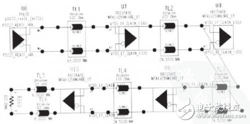
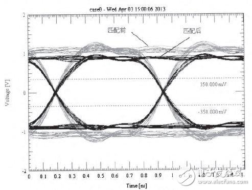
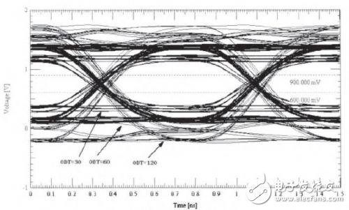
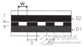
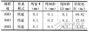
1 Overview Today's computer system DDR3 memory technology has been widely used, data transmission rate has been repeatedly improved, has now reached 1866Mbps. Under such high-speed bus conditions, to ensure the reliability of data transmission quality and meet the timing requirements of parallel bus, the design is realized A great challenge was raised. This paper mainly uses Cadence's time domain analysis tool to quantify the DDR3 design, introduces the main factors affecting signal integrity, analyzes the timing of DDR3, improves and optimizes the design by analyzing the results, improving signal quality and reliability. Security has been greatly improved. 2 DDR3 Introduction DDR3 memory is similar to DDR2 memory in that it contains two parts of the controller and the memory, all of which use source synchronous timing, that is, the strobe signal (clock) is not sent by an independent clock source, but is sent by the driver chip. It has a higher data transfer rate than DR2, up to 1866Mbps; DDR3 also uses 8-bit prefetch technology to significantly increase the storage bandwidth; its operating voltage is 1.5V, which guarantees lower power consumption at the same frequency. The DDR3 interface design is difficult to implement. It adopts the unique Fly-by topology and uses "Write leveling" technology to control the internal offset timing of the device. Although it plays a role in ensuring design implementation and signal integrity, it is not comprehensive to realize high-frequency and high-bandwidth storage systems. Simulation analysis is required to ensure design implementation and signal quality integrity. 3 simulation analysis The simulation analysis of DDR3 is based on the combination of the project: PowerPC 64-bit dual-core CPU module is selected, which uses Micron's MT41J256M16HA-125IT as the memory. Freescale P5020 analyzes the processor. The module configuration memory bus data transmission rate is 1333MT/s, and the simulation frequency is 666MHz. 3.1 Preparation before simulation Before the analysis, it is necessary to communicate with the printed board manufacturer according to the impedance of DDR3 to confirm the laminated structure of the PCB. The key to ensuring good transmission line performance in high-speed transmission is continuous characteristic impedance. It is determined that the impedance of the high-speed PCB signal line is controlled within a certain range, making the printed board a "controllable impedance plate", which is the basis of simulation analysis. The DDR3 bus has a single-wire impedance of 50Ω and a differential line impedance of 100Ω. Set the voltage value of the analysis network terminal; the device to be analyzed includes the passive device assignment model; determine the device class attributes; ensure the device pin attributes (input\output, power/ground, etc.)... 3.2 Circuit simulation analysis The content of the pre-simulation analysis is mainly to optimize the circuit design before PCB design, including reducing signal reflection, overshoot, determining the size of the matching resistor, trace impedance, etc., and selecting the most suitable one by analyzing various configurations of passive components. Parameter configuration. Figure 1 Clock line topology (click to enlarge) (1) Differential clock analysis of DDR3 bus It is well known that in differential transmission, all information is transmitted by the differential mode signal, and the common mode signal radiates energy and can significantly increase EMI. Therefore, it is important to ensure the quality of the differential signal, and the generation of the common mode signal should be reduced. lowest. In the analysis of differential clocks, not only the signal quality of itself, but also other signals are sampled with differential clocks, so attention should be paid to their monotonicity, overshoot value, and so on. In this example, the fly-by topology of the differential clock is in series with the address bus. As shown in Figure 1, the processor P5020 drives the clock topology of four DDR3 memory chips, and performs simple resistor matching at the terminal to differentiate on the PCB. After the trace is taken, reflection analysis is performed to find that the reflected waveform at the receiving end is overshooted. The correct pull-down matching resistor is selected at the output of the processor. Although the voltage amplitude is slightly reduced, the upper and lower overshoots are significantly reduced to eliminate the reflection interference, that is, the common mode component of the differential line is reduced. The results of the comparative analysis are shown in Figure 2. Figure 2: Received DDR3 reflected waveform (2) Verify drive capability and ODT options The driving capability of the DDR3 memory bus data signal is divided into two modes: FULL and HALF. The internal termination resistance (ODT) selection also has 0Ω, 20Ω, 30Ω, 40Ω, 60Ω, 120Ω options, which correspond to different models for controlling signal reflection. influences. In order to improve signal quality and reduce power consumption, the correct parameter model can be selected by analyzing different modes. Take the data bus to analyze different ODT options. Figure 3 is an eye diagram waveform formed by analyzing data signals at different ODT settings. It can be seen from the figure that the higher the ODT impedance, the higher the conversion rate and the larger the amplitude in the case of the same driving excitation and routing; ODT=60Ω, the received signal has the best signal quality, no obvious jitter and overshoot, and the jitter is minimal. Figure 3 data signal eye waveform Usually crosstalk refers to undesired voltage noise interference caused by electromagnetic coupling to adjacent transmission lines as the signal propagates over the transmission line. It generates forward crosstalk and backward crosstalk, which mainly affect the signal waveform above the amplitude and edges. Three adjacent lines are extracted from the DDR3 data bus, the middle one is the attacked network, and the other two are attack networks. The 3-wire model is used for analysis. The following lines are arranged in the following figure. The victim line is low in the middle line. Ping, the attack line on both sides, using 128-bit pseudo-random code, crosstalk analysis according to the different line width and line spacing of the trace, see the analysis results as shown in Table 1. Figure 4 trace cross-section Table 1 crosstalk analysis results It can be seen from Table 1 that the larger the spacing, the smaller the crosstalk effect. Here we follow the 3W principle that the trace edge spacing S is three times the line width W and will greatly reduce the influence of crosstalk. However, the increase in pitch will sacrifice wiring space, so it is necessary to comprehensively consider routing optimization in a limited space. Mini LED Downlight includes round and square two shape frame. We are the manufacturer of producing energy saving interior lighting. This type of down light is made by PC material in frame and aluminum back cover. It has aluminum heat sinking and concealed mounted installation. There are three color temperatures with cool white, warm white and natural white of down lights. There are four colors Red/Blue/Green/Pink. The unique features of led downl light are: CRI>80, PF>0.5. These down lights LED are mainly apply to home, office and school and so on. Mini LED Downlight Commerial LED Downlight,Best LED Downlights,Sustainable Lighting Design Jiangmen Lika Lighting Electrical Appliances Co., Ltd , https://www.lika-led.com