LED optical performance based on microlens array
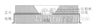
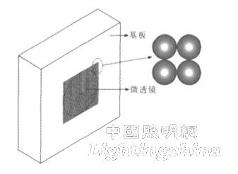
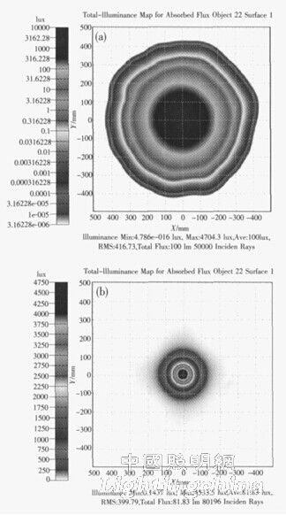
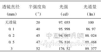
1 Introduction LED is considered to be a new generation of green lighting source due to its all-solid, environmentally friendly and many other advantages. Power LEDs have to enter the field of lighting to achieve daily lighting in the home. There are still many problems to be solved, the most important of which is luminous efficiency. At present, the lumen efficiency of power LEDs is far below the requirements of household daily lighting. Most of them are used for special lighting. In order to improve the luminous efficiency of LEDs, on the one hand, the advancement of chip technology is required; on the other hand, the packaging structure is improved, especially The secondary optical design further enhances the light extraction efficiency. A microlens generally refers to a microlens having a diameter of 10 to 100 μm, and a series of microlenses are regularly arranged to be a microlens array (MLA). In recent years, people have used MLA technology to improve the light extraction efficiency of LEDs, and have done a lot of research [1~4]. DongwooKim et al [5] used plasma etching technology to obtain 10μm MLA, which can increase the LED light intensity by 40%. In this paper, a typical LED package structure is studied. By installing a microlens array on the light exit surface, the light distribution is improved, and the influence of the microlens array on the optical performance of the LED is explored, and good results are obtained. 2 LED package model design The model design of the LED package is shown in Figure 1. The LED chip is glued on the metal substrate with silver glue, the chip electrode is led out by the gold wire, the surface of the reflector cup is metallized to increase the reflection effect, and the inner chip is sealed with a silicone rubber to protect the chip and the Lead Wire. The structural dimensions of each part are: substrate 7 mm × 7 mm, chip 1 mm × 1 mm × 0.25 mm, reflector cup bottom radius 0.8 mm, top radius 1.5 mm, inclination angle 55 °. After finite element software ANSYS simulation, the highest temperature of the package structure appeared in the LED chip, reaching 76 ° C, the lowest temperature appeared on the upper surface of the silica gel, 25 ° C, which can meet the requirements of the device for heat dissipation performance. Figure 1 LED model design 3 microlens array design Microlens arrays have a wide range of applications in micro-optical systems. However, conventional optical components are generally large in size, typically on the order of millimeters and above. For example, lenses and prisms made by glass cold-working technology are more than 1 mm in diameter due to process limitations, and lenses having smaller diameters (such as tens of micrometers) are produced. This process is generally impossible. In order to make microlenses, conventional machining methods cannot be used, and newly developed optical micromachining methods must be employed. The development of microlens arrays was mainly in the 1980s. On the basis of microelectronics technology, optical micromachining technology developed rapidly, and a series of new processes for making microlens arrays appeared. At present, the microlens processing methods reported in the literature include a reflow method [6], an em-bossing method [7], a droplet method [8], a gray scale method (gray scale) method. [9], etching (etching) method [10] and the like. LED light sources for illumination are moving toward high power. However, there are currently problems such as low light extraction efficiency. The tremendous advancement in optical component fabrication technology has opened up a new path to solve this problem. Fig. 2(a) shows a conventional method for concentrating light through a large-sized lens, but this method is not suitable for multi-chip LEDs; and Fig. 2(b) is a method using micro-optical elements, which can satisfy miniaturization, Low cost, high performance requirements. Heptagon's refractive and diffractive hemispherical MLAs produced using the unique REEMO technology have the advantages of low cost, good durability and easy mass production [11]. Figure 2 Optical lens components for LEDs 3 is a three-dimensional view of a light-emitting surface mounted microlens array, which is a refractive hemispherical lens in which the microlens has a diameter of 0.1 mm, an effective aperture ratio of 78.5%, and a total light exit surface of 31×31 array. Figure 3 Microlens array model design 4 Optical simulation and analysis TracePro is a widely used optical design and analysis software. This article uses TracePro to perform simulation experiments on the designed LED model. The package model designed in Figure 1 and Figure 3 is imported into TracePro to establish a light distribution model, and parameters such as surface properties and chip luminous flux can be defined for simulation. The light-emitting surface is provided with 50,000 light rays, the luminous flux is 100 lm, the inner surface of the reflective cup is a mirror surface, that is, the reflectivity is 100%, and the microlens is a transparent synthetic resin having a refractive index of 1.493. The LED package structure model is assumed as follows: the light emitted from the chip is not lost, and the Lambert distribution is satisfied; the inner surface of the reflector cup is ideal for total reflection; the absorption of photons and the effects of electrical properties and temperature are not considered. Figure 4 is a simulated light intensity distribution map. It can be seen from the figure that the angle of light emission is small, which depends mainly on the cup depth and inclination of the reflector cup. Oliver Kuckmann [12] studied the packaging technology of high-power LED arrays and found that to increase the luminous efficiency of LEDs, reflection The design of the components is very important. The general method is to mount the lens directly on the LED. There is also a design of additional secondary optics, depending on the optical requirements of the package. In Fig. 4(a), the light intensity distribution is narrow, the illuminance intensity changes uniformly with the angle, and the center illuminance intensity is the largest, which is the result of the condensing cup concentrating; Fig. 4(b) after the microlens array is mounted, the light intensity is distributed into an ellipse. The shape has a half-intensity angle of 40°, and the luminous intensity changes little with angle, and the light is diverged compared with (a), which is caused by the redistribution of light by the secondary refraction of the microlens. Fig. 4 Light intensity distribution map (a) Original model light intensity distribution map; (b) Microlens array model light intensity distribution map Figure 5 is a simulated illuminance distribution map. In the simulation, a receiving screen is set at a distance of 100 mm from the LED, and the screen size is 1000 mm × 1000 mm × 1 mm, and the side of the LED light is set to be completely absorbed, and the illuminance map displayed on the screen is obtained. As can be seen from the figure, the illuminance is uniformly distributed in a stepwise manner. Fig. 5(a) has a spot diameter of about 800 mm, the center illuminance is the highest, which is 10000 lux, and Fig. 5 (b) has a spot diameter of about 240 mm and a central illuminance of 4,750 lux. If the same diameter is 200mm, the illuminance is almost the same, but the illuminance of the former is attenuated by 90%. After installing the microlens array, the illuminance is attenuated by 78.9%, and the illuminance attenuation is reduced by more than 12%. Although there is attenuation, it is obviously excellent. In the former, all the light is distributed over a smaller area, so the microlens array is very significant for increasing the illuminance. Figure 5 illuminance diagram (a) original model illuminance diagram; (b) microlens array model illuminance diagram Table 1 shows the effect of different lens sizes on the optical performance of the LED. Compared with the lensless lens, the light intensity and the luminous flux are reduced. This is the absorption and refraction of the transparent resin, which consumes a part of the light and impurities. Caused by the presence of astigmatism. By changing the size of the lens, it was found through simulation that the smaller the diameter of the microlens, the greater the light intensity and the smaller the luminous flux. This is because the smaller the diameter of the microlens, the larger the number of microlenses on the light-emitting surface, which tends to increase the loss of luminous flux, but the luminous flux (ie, light intensity) in a unit solid angle increases. If the light exit surface is added with a lens with a diameter of 3 mm, the light intensity is increased, but the center light intensity is small, the surrounding light intensity is large, and the spot is prone to occur. The reason for this may be related to the design of the reflector cup, and further research is needed. Table 1 Effect of lens size on optical performance of LED 5 Conclusion As the main device in the field of micro-optics, microlens arrays have important applications in concentrating, beam conversion, optical imaging and so on. The combination of semiconductor process technology and various micro-optical components can form a complete micro-optical electromechanical system (MOEMS), which can be used for functions such as splitting, beam deflection, focusing, switching, etc., and is widely used in backlight modules such as LCDs, projections. Optoelectronic and communication products such as machines and optical fiber communication systems. In this paper, an LED optical system using microlens array is designed according to the illuminating characteristics of LED. The influence of microlens array on the optical properties such as LED light intensity and illuminance is studied. The simulation results show that the LED optical system based on microlens array can be improved. The light extraction efficiency, light intensity distribution and illuminance distribution of the illumination system can reduce the illumination attenuation of the LED by more than 12%, thereby obtaining a more uniform illumination system. Edit: Cedar
Taillight Wire Harness apply in automotive,motocycle,bus,bike,truck.
Yacenter
has experienced QC to check the products in each process, from developing
samples to bulk, to make sure the best quality of goods. Timely communication
with customers is so important during our cooperation.
If you can't find the exact product you
need in
the pictures,please don't go away.Just contact me freely or send your sample
and drawing to us.We will reply you as soon as possible.
Tail Light Wiring Harness,Trailer Wiring Harness,Trailer Light Wiring Kit,Trailer Light Harness Dongguan YAC Electric Co,. LTD. , https://www.yacenter-cn.com