Abstract: This applicaTIon note analyses the parameters that affect the errors in precision digital-to-analog converter (DAC) applicaTIons. The analysis focuses on the factors introduced by both the data converter and the voltage reference. It describes the calculaTIons required to select the data converter and the reference to meet the system's target specificaTIons. The calculations are available in a spreadsheet.
OverviewWhen designing a digital-to-analog converter (DAC) system, the DAC specifications and its voltage reference work in tandem to produce the overall system performance. Consequently, selection of both DAC and reference should be made together. The components' specifications can be traded off against each other to ensure that system specifications are met at the lowest cost.
This application note focuses on Maxim's 3-terminal voltage references and precision DACs. To design a system, one must first understand how the parts are specified and then how their performance characteristics interact. Voltage references and DACs have many specifications. Only those factors relevant to the error budget will be discussed here.
Voltage Reference Specifications Initial AccuracyThis is the output voltage tolerance, ignoring any effects of temperature, input voltage, and load. Temperature is normally + 25 ° C.
Output-Voltage Temperature CoefficientThis is the change in reference output voltage, measured for a given change in temperature and specified in ppm / ° C. Maxim uses the box method. The shape of the change vs. temperature characteristic is not specified; only the limits of this function are specified. The limits of the output voltage do not necessarily coincide with the limits of temperature. So, to calculate the maximum change, multiply the temperature coefficient by the temperature range for the part. Thus to illustrate, if a part has a temperature coefficient of 5ppm / ° C, specified from -40 ° C to + 85 ° C, the maximum deviation over temperature would be:
ΔV = (TMAX-TMIN) × TC = (85 + 40) × ± 5 = ± 625ppm
It is generally best to select a device that is specified over the required temperature range, rather than a broader range. For instance, the MAX6025A is specified as a 15ppm / ° C reference over 0 ° C to + 70 ° C. This reference value works out to 1050ppm over the range. If, however, one chose a reference specified over the -40 ° C to + 85 ° C range, a reference that is 1050/125 = 8.4ppm / ° C or better would be required. Note that some devices are specified over several temperature ranges.
A graphical example of the box method is shown in Figure 1. Two different example curves are shown, both of which satisfy the 5ppm / ° C specification over -40 ° C to + 85 ° C.
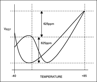
Figure 1. Example temperature characteristics.
With series references, therefore, it is generally not possible to relate voltage drift and temperature so that one can calculate the drift over a specific range other than that over which the part is specified.
Line Regulation This term defines the incremental change in output voltage for a change in input voltage. It is normally defined in terms of µV / V.
Load Regulation This term defines the incremental change in output voltage for a change in load current. Some DACs may not buffer the reference input. Therefore, as the code changes, the reference input impedance will also change, causing a change in reference voltage. This change is generally small, but should be considered in high-accuracy applications. Note that this is more important with some DAC topologies such as R-2R ladders, while resistive string topologies are less susceptible.
Temperature HysteresisThis is the change in reference voltage at + 25 ° C after the temperature is cycled from TMIN to TMAX. It is specified as a ratio of the two voltages and expressed in ppm:
TEMPHYST = 106 × (ΔVREF / VREF)
Where ΔVREF is the change in reference voltage caused by the temperature cycle.
Long-Term StabilityThis is the change in reference output voltage vs. time, specified in ppm / 1000 hours. Cumulative drift beyond a 1000-hour interval is not generally specified, but is usually much lower than the initial drift. An application's long-term stability can be improved by PCB-level burn-in. A typical output-voltage long-term stability characteristic is shown in Figure 2.
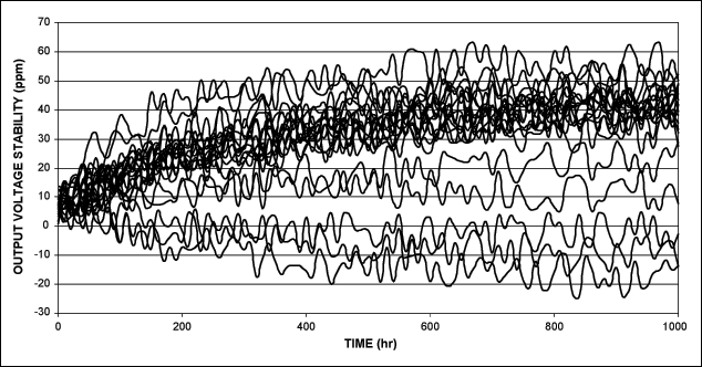
Figure 2. Typical output-voltage long-term stability.
Output Noise VoltageThis defines the voltage noise at the reference output. The 1 / f component is specified in µVP-P over a 0.1Hz to 10Hz bandwidth, and the wideband noise is usually specified in µVRMS over a 10Hz to 10kHz bandwidth.
DAC SpecificationsOnly buffered-voltage-output DACs are discussed here, as the key points about error calculations are easier to illustrate with this architecture. Current-output DACs are typically used in a multiplying configuration (MDAC) to provide variable gain; they usually require external op amps to buffer the voltage generated across a fixed resistor.
Focusing discussion on the reference voltage, the main characteristic of this DAC architecture is the varying DAC reference input resistance vs. DAC code. Many DACs are implemented using an R-2R ladder. The resistance of the ladder will change with DAC code. If the reference drives the ladder directly, the reference must have sufficient load regulation to avoid introducing errors. Care must be taken to ensure that the voltage reference can source enough current at the DAC's minimum reference input resistance. Note that some DAC configurations will draw virtually zero current from the reference at DAC code 0. Hence, switching from code 0 to code 1 can create a large current transient in the reference.
Two other DAC specifications are important to voltage-reference selection: reference-input-voltage range and DAC output gain. These specifications will define the reference voltage for the particular application.
Output Error and Accuracy SpecificationsOutput error is defined as the deviation from an ideal output voltage that would be provided by the perfect match of voltage reference and DAC. It is important to note that this article addresses absolute accuracy, meaning that everything is referenced to an ideal DAC output-voltage range. For example, a 12-bit DAC code 4095 should produce an output of 4.096V with a reference voltage of 4.096V; any deviation from this is an error. This performance contrasts to relative accuracy, where the full- scale output is defined more by the application than by an absolute voltage. Consider another example: a ratiometric system where an ADC and a DAC with equal resolution share a reference. It may not matter (within reason) what the actual reference voltage is, as long as the DAC-output and ADC-input voltages are nearly equivalent for a given digital code.
Output error is often specified as a one-sided value (in LSBs at the DAC resolution), but it actually implies a double-sided error (Figure 3). For example, a 12-bit DAC with a 4.096V output range has an ideal LSB step size of 4.096V / 4095 ~ 1mV. If the specified output error in this case is 4 LSBs at 12-bit resolution, this means that the DAC output at any code could be ± 4 LSBs (or ± 4mV) from the ideal value. Consequently, accuracy is defined by how many actual bits are available to reach a desired output voltage with at most 1 LSB of error: Accuracy = DAC Resolution-log2 (Error) So in this example: Accuracy = 12-log2 (4 ) = 10 bits Therefore, one can only get to within 1 LSB at 10-bit resolution (± 4mV = ± 4/4096 = ± 1/1024) of any ideal DAC output value.
Sources of system gain error include: Reference initial error Reference-output temperature coefficient Reference temperature hysteresis Reference long-term stability Reference load regulation Reference line regulation Reference output noise DAC gain error DAC offset error DAC gain-error temperature coefficient Other sources of system error include : DAC integral nonlinearity (INL) DAC output noise
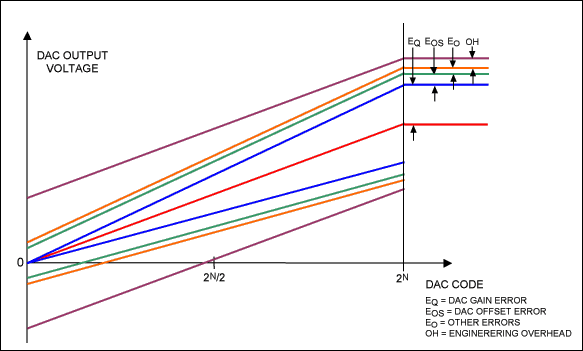
Figure 3. Data show how errors compound to define the system DAC transfer function.
Although the target error applies over the entire DAC code range, most of the error sources mentioned above cause an effective gain-error variation that is largest near the full scale (highest DAC codes) of the transfer function (Figure 3). Gain errors reduce with decreasing DAC code value; these errors are halved at midscale and virtually disappear near code zero, where offset error dominates. Error sources that do not exclusively affect the gain error and apply equally over most of the DAC code range include DAC integral nonlinearity (INL ) and output noise.
INL is typically defined using one of two methods: absolute linearity or end-point linearity (Figure 4). The offset error is removed and the gain error is normalized before the INL is measured. Absolute linearity compares the DAC linearity to the ideal transfer- function linearity. End-point linearity uses the two measured end points to define the linearity (a straight line is drawn between these points); all other points are compared to this line. In either case, INL should be included in the error analysis. In the latter case, the DAC INL error is zero at the end points, but can be present at DAC code words just inside these values. As an example, for a 12-bit DAC with INL defined between the end points of 0V and 4.095 V (full scale), the INL specification applies to DAC codes near 0 and 4095. For maximum error calculations, it is reasonable to add the DAC's INL and noise-induced output errors to the previously mentioned gain errors that are most severe near code 4095 . Some DACs are sp ecified with differing INL values ​​over the range of codes. DACs are often used in applications where the whole code range is not used, and devices specified in this way can provide better performance over a smaller code range.
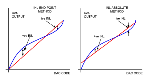
Figure 4. DAC INL measurement.
DAC and Reference Design Examples To illustrate the steps involved with voltage reference selection for DACs, a few design examples cover a range of applications (Table 1). The design steps are broken into individual sections by design examples (ie, Design A through Design D) . A spreadsheet was developed to calculate the various steps and produce the results. In the spreadsheet, cells with blue text should be entered by the designer. Cells with red text show calculated results.
Table 1. Requirements for DAC Design Examples
| Parameter | Design A | Design B | Design C | Design D |
| Main Design Objectives | Low cost, loose accuracy | High absolute accuracy and precision | One-time calibrated, low drift | Low voltage, battery powered, moderate accuracy |
| Example Application | Consumer audio device | Lab instrument | Digital offset and gain adjustment | Portable instrument |
| DAC | MAX5304, 10-bit single | MAX5170, 14-bit single | MAX5154, 12-bit dual | MAX5176, 12-bit single |
| Minimum Reference Input Resistance | 18kΩ | 18kΩ | 7kΩ (two shared 18kW inputs) | 18kΩ |
| Output Voltage | 0 to 2.5V | 0 to 4.096V | 0 to 4.000V | 0 to 2.048V |
| DAC Output | Force / sense | Fixed gain = 1.638 | Fixed gain = 2 | Fixed gain = 1.638 |
| Power Supply | 5V (varying)
4.5V (min),
5.5V (max) | 5V (constant)
4.95V (min),
12V available | 5V (constant)
4.75V (min),
5.25V (max) | 3V (varying VBatt)
2.7V (min),
3.6V (max) |
| Temperature Range | 0 ° C to + 70 ° C
(commercial) | 0 ° C to + 70 ° C
(commercial) | -40 ° C to + 85 ° C
(extended) | + 15 ° C to + 45 ° C
(<commercial) |
| Signal Bandwidth | 10Hz to 10kHz | DC to 1kHz | DC to 10Hz | 10Hz to 10kHz |
| DAC Calibration | None | Burn-in, plus annual
(gain and offset) | One-time factory
(gain and offset) | None |
| Maximum Target Error | 16 LSB at 10 bits
(6-bit accuracy) | 2 LSB at 14 bits
(13-bit accuracy) | 4 LSB at 12 bits
(10-bit accuracy) | 8 LSB at 112 bits
(9-bit accuracy) |
Step 1. Voltage Ranges and Reference Voltage DeterminationWhen selecting a voltage reference for a DAC application, the first task is to evaluate the supply-voltage and the DAC's output-voltage ranges. A section of the spreadsheet is shown below (Figure 5). To simplify the design examples described above, DACs have already been chosen, so their output gain is not a variable that one would trade-off in a real design.
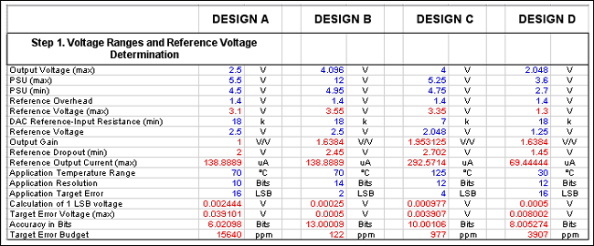
Figure 5. The error calculation spreadsheet assists in balancing the tradeoffs between a DAC and voltage reference.
First, enter the values ​​for the maximum output voltage and power-supply range. Some DACs do not allow the reference input to go all the way to the power-supply rails, so the reference overhead can be entered. In addition, enter the minimum DAC input resistance. Thus there are four calculated parameters that can be used for reference selection: maximum reference voltage, minimum dropout, and maximum steady-state output current. In addition, one can use the maximum power-supply voltage, as this will determine the maximum power-supply voltage which the reference can accept. The calculated output gain is often provided by an external op amp, but may be internal as in Design B.
Design A. Low Cost, Loose AccuracyFor the Design A example, VDD is 5V and the output range is 0 to 2.5V. Thus, a 2.5V reference is used and the MAX5304 force / sense output is set to unity gain (OUT and FB pins shorted). A lower voltage reference could be used with a higher, externally set gain, but the approach here saves the two resistors for a low-cost design.
Design B. High Accuracy and PrecisionA 2.5V reference is chosen for the Design B example. The MAX5170 gain is fixed at 1.638 and a final output voltage range of 0 to 4.096V is required. If a lower reference voltage is desired for Design B, a MAX5171 DAC could be used and its output force / sense gain could be set higher than 1.638 with external resistors. Note that the minimum VDD level is 4.95V. Thus the highest reference voltage that could be used is 4.95V-1.4V = 3.55 V, as the DAC reference input is limited to (VDD-1.4V).
Design C. One-Time Calibrated, Low DriftIn the Design C example, the MAX5154 has a fixed gain of 2, so a 2.048V reference provides a nominal 4.096V output at full scale. This voltage must exceed the 4.000V design requirement, so that a gain calibration can be used to scale the voltage down to the 0 to 4V range. This design also has other reference voltage options if the MAX5156 force / sense DAC is used. Note that the reference-input upper-limit voltage is 4.75V -1.4V = 3.35V.
Design D. Low Voltage, Battery Powered, Moderate AccuracyThe minimum VDD is 2.7V in the Design D example, so the largest reference voltage that could be used is 2.7V-1.4V = 1.3V. For this example, a 1.25V reference satisfies the 0 to 2.048V output range, as the MAX5176 gain is 1.638. It is important that the worst-case reference voltage, including all error terms, remains below 1.3V, or the specification for the DAC reference input voltage will be exceeded. Approximate dropout voltages were calculated for each of the design examples (Figure 5). All of these voltages are well above the 200mV (or lower) dropout voltages typical of Maxim's voltage references. Because the upper-reference input voltage of most Maxim DACs is limited to VDD-1.4V, the dropout voltages can normally be ignored with these designs if, that is, the DAC and voltage reference use the same positive supply rail. The dropout voltages are approximate, because they were calculated without any error terms such as initi al accuracy. Nonetheless, these errors are small compared to typical dropout voltages, and they can be ignored.
Step 2. Initial Voltage Reference Device-Selection Criteria There are many factors to consider when selecting the optimal reference for each design. To make the procedure manageable, candidate devices will be identified based on: the reference voltage determined above; an estimate of required initial accuracy ; an approximated temperature coefficient; and the reference output current needed for the chosen DAC. These selection criteria are shown in the spreadsheet segment below (Figure 6). Other factors such as cost, quiescent current, packaging, and a quick glimpse at the remaining specifications will be used to select a specific initial device for each design. The remaining specifications will be analyzed in Step 3 to determine if the devices satisfy the overall accuracy requirements.
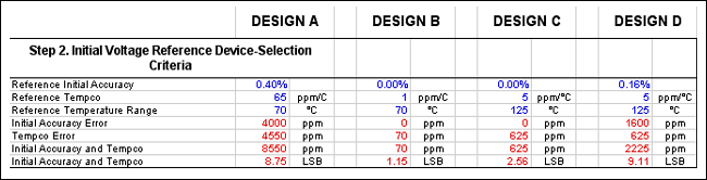
Figure 6. This portion of the spreadsheet identifies the criteria for selecting the optimal reference for a design.
Design A. Low Cost, Loose AccuracyA 2.5V reference was chosen in Step 1 above. The MAX6102 is a very low-cost 2.5V reference, specified with 0.4% initial accuracy and 65ppm tempco over the commercial temperature range. It looks as though this could be a good choice for this application. The spreadsheet shows an initial accuracy and tempco error of 8.4 LSB, which is well within the 16 LSB requirement.
Design B. High Accuracy and PrecisionBecause Design B has such challenging accuracy requirements, the MAX6225 and MAX6325 buried-zener references are the initial candidates. These references have low temperature coefficients, excellent long-term stability, and low noise. These devices also have very good initial accuracy, but this specification is unimportant in the case of Design B, because gain errors caused by the DAC and the voltage reference are calibrated out. Therefore, one can set the reference initial tolerance to zero in the spreadsheet. The MAX6225 and the MAX6335 source 15mA, so driving the MAX5170 DAC reference input (2.5V / 18k ~ 140µA, max) is not an issue. The MAX6325 is chosen because it has the only tempco (70 ° C × 1ppm / ° C = 70ppm, max) that is beneath the overall 122ppm accuracy requirement (2 LSB at 14 bits = 2/214-1 = 2/16383 = 1.22 × 10-4 = 122ppm) while leaving margin for the other error sources. If the Design-B accuracy requirements are relaxed slightly, the MAX6225 A-grade device (2ppm / ° C, max, tempco) would reduce the reference cost by more than half.
A 12V supply is conveniently present in the Design-B example. This requirement allows use of the MAX6325, which needs an input voltage of at least 8V. If 8V (or higher) is not available in the system, the MAX6166 (A grade) or MAX6192 (A grade) bandgap-based references could be considered, but a slight relaxation of the system specifications would be required.
Design C. One-Time Calibrated, Low DriftThe MAX6162 and MAX6191 A-grade devices are considered for Design C because of their low tempco (5ppm / ° C max): Total error budget is 4 LSB at 12 bits = 4/4096 × 106 = 977ppm
Required tempco ≤ 977ppm / (85-(-40)) ≤ 7.8ppm / ° C
Available error beyond tempco = 977ppm-5ppm / ° C × 125 ° C = 352ppm Note that the MAX6162 and the MAX6191 both have 2mV (977ppm) initial accuracy. This specification is not a concern with the 2.048V reference, because the output-voltage range is only 0 to 4.000V and a gain calibration is planned for this design. The reference initial accuracy is set to zero in the spreadsheet. The MAX6162 (5mA of output current drive) and the MAX6191 (500µA of output current drive) can both drive the 293µA reference input current that results when the two MAX5154 DAC reference pins are tied together (2.048V / [14kΩ || 14kΩ]). However, the MAX6162 has more margin if additional loads are connected to the reference output. The MAX6162 does have higher quiescent current than the MAX6191 (120µA versus 35µA, max), but this is not a deciding factor as Design C is not power constrained. After reviewing the initial specifications, it is clear that either device is probably acceptable. However, the MAX6162 is the first choice due to its higher output current. If further analysis shows the MAX6162 to be marginally unacceptable, the MAX6191 could be considered because it has slightly better load-regulation, temperature-hysteresis, and long-term-stability specifications.
Design D. Low Voltage, Battery Powered, Moderate AccuracyFollowing the approaches used in the other examples, the total error for Design D is found to be 3907ppm (106 × 16/4095). Over the narrow + 15 ° C to + 45 ° C temperature range, a tempco of at most 130.2ppm / ° C (3906ppm / 30 ° C) can be tolerated. However, one must be careful not to make a common mistake here. Remember that these example exercises are dealing with the box method. So start again and ignore the 130ppm / ° C that was just erroneously calculated. Using the guideline from Design A to allocate roughly half of the error budget to the tempco, then reasonable, conservative reference choices are the MAX6012 (A and B grades are 15ppm / ° C and 25ppm / ° C, respectively, over 0 ° C to + 70 ° C) and the MAX6190 (A, B, and C grades are 5ppm / ° C, 10ppm / ° C, and 25ppm / ° C, respectively , over -40 ° C to + 85 ° C). These parts are considered because they have a maximum quiescent current of 35µA, which is appropriate for the low-power needs of Desi gn D.
The MAX6190C price is in the same range as the MAX6012B. Either part will probably work in the application. However, the MAX6012A is especially attractive, because it is available in a 3-pin SOT23 package, which is ideal for a small, battery- powered, portable instrument.
A quick check of the MAX6012A reveals the tempco-related error to be 1050ppm (70 ° C × 15ppm / ° C). The initial error of 3200ppm (0.32%) also needs to be considered, as there is no trimming planned for this design . The sum of these two errors is 4250ppm, which is already outside the 3906ppm design limit. Because the MAX6012A is insufficient, the 3-pin SOT23 package is abandoned. The MAX6190A is chosen as a starting point, because its initial error of 1600ppm and 5ppm / ° C leave enough room for the other error terms. Reference output current is not a concern for this design, because the MAX6190 can supply 500µA (>> 69µA design requirement).
Step 3. Final Specification Review and Error-Budget AnalysisWith the preliminary selection of references complete, it is now time to verify the remaining specifications, which include reference-load regulation; input-line regulation; output-voltage temperature hysteresis; output-voltage long -term stability; and output noise voltage. The analysis is shown in the spreadsheet segment below (Figure 7).
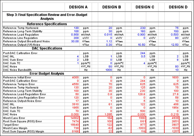
Figure 7. This portion of the spreadsheet helps calculate the remaining specifications and, ultimately, the error budget.
Each example is analyzed, focusing on the specifications that apply to that particular design. It is most convenient to do the error-budget accounting in parts per million (ppm), although this could be done equivalently in other units such as%, mV, or LSBs. It is also important to apply the proper scaling and to use the proper normalization factor to obtain the correct error values. Reference-error terms can be calculated relative to the reference voltage or the DAC output voltage. For example, assuming a reference error of 2.5mV (eg, noise, drift, etc.) and a reference voltage of 2.5V, then: Reference output error = 106 × 2.5mV / 2.5V = 1000ppm Assuming that the DAC output amplifier has a gain of 2.0, then both the error and the reference voltage are scaled. This produces the same result at the DAC output (5V full-scale range): DAC output error = 106 × (2.5mV × 2) / (2.5V × 2) = 1000ppm Into this section of the spreadsheet, enter the reference specifications for: temperature hysteres is, long-term stability, load regulation, line regulation, and output noise. Also enter DAC specifications for: INL, gain error, gain tempco, and noise.
The spreadsheet will calculate values ​​for: worst-case error, root-sum-square (RSS) error, worst-case error margin, and RSS error margin. It is important to think of how the errors can stack up. Some very accurate applications may be very difficult to meet if a worst-case analysis is used. If one can assume that errors may not be correlated, then the RSS method can often be used. Yet, theoretically, some boards that result may not be as accurate as they should be.
Design A. Low Cost, Loose AccuracyNo calibration or trimming is planned for Design A, so the MAX6102 initial error of 4000ppm (or 0.4%) directly becomes part of the budget, as does the 4450ppm due to the voltage-reference tempco (70 ° C × 65ppm / ° C). The typical MAX6102 output-voltage temperature-hysteresis specification is also used directly in the error budget. (Remember that this is a typical value, if the design ultimately has marginal accuracy.) For output-voltage long -term stability, assume twice the MAX6102 1000-hour specification (2 × 50ppm = 100ppm). This is fairly conservative, as it is usually much better after the first 1000 hours. A conservative estimate here at least partially offsets the typical specification used for temperature hysteresis.
To calculate the variation in reference voltage caused by load regulation, one must know the worst-case range of currents that the voltage reference supplies to the DAC's reference input. Recall that in Step 2 above, the maximum DAC reference current that the MAX6102 would have to drive is 140µA. The minimum current is close to 0 since the MAX5304 in an R-2R ladder. The MAX5304 reference input is effectively an open circuit (several GΩ input impedance) when the DAC code value is 0. This means that the total output-current variation that the MAX6102 sees is 140µA. This value should be used for the load-regulation calculation:
| Load-regulation error | = 140µA × 0.9mV / mA | = 126µV (max) |
| = 106 × 126µV / 2.5V | = 50ppm (max) |
In general, it is best to be conservative and use the maximum output current directly for the load-regulation calculation. There is a possible exception: if you are trying to extract the last bit of accuracy from a design and both the maximum and minimum DAC reference input resistance values ​​are well specified. This approach results in a smaller load-regulation error because of the smaller ΔIREF.
Because the power supply is specified as varying for this example, one must consider the effects of input line regulation on the MAX6102 reference. The power-supply range is specified as 4.5V to 5.5V. From this, a conservative reference-voltage line- regulation calculation is possible:
| Load-regulation error | = (5.5V-4.5V) × 300µV / V | = 300µV (max) |
| = 106 × 300µV / 2.5V | = 120ppm (max) |
The final voltage-reference-related error term to consider is the effect of reference output-noise voltage. Conveniently, Design A has a signal bandwidth (10Hz to 10kHz) that corresponds to the exact MAX6102 noise voltage bandwidth. Consequently, the wideband noise- voltage specification of 30µVRMS is used directly (that is, bandwidth scaling is not required). Comparing the load- and line-regulation values ​​(126µV and 300µV, respectively), it is apparent that noise is not a major contributor in this design. Using crude approximations to get numbers for the error analysis, one can assume an effective peak noise value of ~ 42µV (30µV × √2), which corresponds to 17ppm (106 × 42µV / 2.5V) with the DAC gain of 1. This analysis is trying purposefully to keep the noise calculations simple; a more detailed analysis can be performed if the relative error of the noise is larger or if the design is marginal. Remember that noise is specified as a typical value when judging design margin.
Consider now the relevant MAX5304 DAC specifications that impact accuracy at, or near, the upper end of the code range. The DAC INL value of ± 4 LSB (at 10 bits) is used directly. Treating it as a single-sided quantity, as with the other error terms in our analysis, one arrives at a value of 3910ppm (106 × 4/1023). Similarly, the DAC gain error is specified as ± 2 LSB and results in an error of 1955ppm (106 × 2/1023) . The final MAX5304 DAC specification to be considered is gain-error tempco, which gives a typical error of 70ppm (70 ° C × 1ppm / ° C). The DAC output noise is not specified for the MAX5304, so it is ignored, probably without adverse consequences in this 6-bit-accurate system.
When all of the error sources are summed, the result is a worst-case error of 14902ppm which, although fairly close, meets the target-error specification of 15640ppm. When confronted with this marginal situation, one can rationalize that the design will probably never have an error of this magnitude, because the error specification assumes worst-case conditions for most parameters. The RSS approach gives an error of 7474ppm, which is valid if the errors are uncorrelated. Some error sources may be correlated, so the truth probably lies somewhere between these two numbers. But regardless of the approach, the Design-A requirements have been met.
Design B. High Accuracy and PrecisionThe initial error of the A-grade MAX6225 is 0.04% or 400ppm, which exceeds Design B's entire 122ppm error budget. Because this application has gain calibration, virtually all of this reference initial error can be removed. This latter decision assumes that the calibration equipment has sufficient (~ 1µV) accuracy and the trim circuit has enough precision. The tempco contribution is calculated as 70ppm (70 ° C × 1ppm / ° C), and the typical temperature hysteresis value of 20ppm is used directly . The long-term stability specification of 30ppm is also used rather than a more conservative number, because the instrument in this application has an initial burn-in as well as an annual calibration.
Applying the same assumptions used in Design A, then Design B's reference output current variation is 140µA (coincidentally, the same number as in Design A). In this case, the MAX6225 data sheet specifies the load regulation in ppm / mA. To use the spreadsheet, convert this value to mV / mA, which leads to the following load-regulation error calculation:
| Load-regulation error | = 6ppm × 2.5 / 1000 | = 0.015mV / mA |
| = 140µA × 0.015mV / mA / 2.5 | = 0.8ppm (max) |
The power supply is specified as constant in this application, so the line regulation is assumed to be 0ppm. The precise bounds are not defined, but this does not matter since calibration will remove any errors. Note that it would be <1ppm even if the power supply were not constant, as long as the regulation remains within the specified 4.95V to 5.05V range, because the MAX6225 line-regulation specification is 7ppm / V max. Hence, zero is entered into the spreadsheet.
Because the bandwidth for Design B is specified as DC to 1kHz, one must consider both the 1.5µVP-P low frequency (1 / f) noise and the 2.8µVRMS broadband noise specified from 0.1Hz to 10Hz and 10Hz to 1kHz, respectively. Using the same crude RMS-to-peak approximation as Design A, and adding the two peak-noise terms together, the total noise estimate is 2ppm at the reference output ([[0.75µV + 2.8µVRMS × √2]/2.5V] × 106). Again, to put the values into the spreadsheet, convert to ppm. Notice that this is the same value that one would obtain if it were calculated at the DAC output. This is because the equation would be multiplied by 1.638/1.638 to rescale everything to 4.096V. It is worth mentioning that the peak-noise-sum method used here is fairly conservative, yet the total error contribution is still relatively small. An RSS approach is probably more accurate, because the two noise sources are most likely uncorrelated. Still, this smaller value would be even more "in the noise" compared to the peak-value approach.
All that remains for the Design-B analysis is to include the DAC error terms. The INL for the A-grade MAX5170 DAC is specified as ±1 LSB, which is 61ppm and exactly half of the 122ppm error budget of ±2 LSB at 14 bits. The DAC gain error is specified as ±8 LSB worst case, but this error is removed completely by the gain calibration mentioned earlier. As with the reference, one can set the gain error to zero in the spreadsheet. The calibration works as follows: The DAC is set to a digital code where the ideal output voltage is known (for example, decimal DAC code 16380 should produce precisely 4.095V at the output). The reference voltage is then trimmed until the DAC output voltage is at this exact value, even if the reference voltage itself is not 2.500V. The MAX5170 DAC does not list a gain tempco, although the gain error is specified over the operating-temperature range. Because the gain error is calibrated out at only one temperature, Design B should be tested to ensure that the gain does not drift excessively over temperature. The final consideration is the MAX5170 DAC output noise, whose typical peak noise is roughly estimated as 1ppm ([106 × √(1000Hz × π/2) × 80nVRMS/

× √2]/4.096V).
Ultimately, the final worst-case accuracy is 184ppm (~ ±3 LSB at 14 bits), which does not quite meet the accuracy target of 122ppm. In contrast, the RSS accuracy is acceptable at 100ppm. Based on these numbers, the design can be considered a success. It has illustrated the important points and is close to the target accuracy with several conservative assumptions. In a real-world application, this design could be accepted as is, or the accuracy requirements could be relaxed slightly. Alternatively, a more expensive reference could be used if this design were not acceptable.
Design C. One-Time Calibrated, Low DriftThe initial error of the A-grade MAX6162 is 0.1%, which consumes the entire Design-C error budget of 977ppm. However, like Design B this is at least partially calibrated out. Note that the uncalibrated +4.096V MAX5154 DAC full-scale output voltage exceeds the required +4.000V output range, and that the DAC has 1mV resolution even though only ±4mV of accuracy is required. Therefore, it is possible to do a digital calibration on the DAC input digital codes to remove some of the reference's initial error and the DAC's gain error.
The digital gain calibration is best demonstrated with an example. Assume that the DAC output voltage needs to be at the full-scale value of 4.000V, but the ideal decimal DAC code of 4000 results in a measured output of only 3.997V due to various errors in the system. Using digital calibration, a correction value is added to the DAC code to produce the desired result. In this example, when the DAC output voltage of 4.000V is required, a corrected DAC code of 4003 is used instead of 4000. This gain calibration is scaled linearly across the DAC codes, so it has little effect at the lower codes and more impact on the upper codes.
The digital gain calibration accuracy is limited by the 12-bit resolution of the DAC, so the best one can expect is ~±1mV or 244ppm (106 × 1mV/4.096V) of error after the calibration has been applied. Note that the accuracy is calculated on a 4.096V scale in this example to maintain consistency. It could be calculated relative to the +4.000V output range if required by the application; the error would be slightly higher.
If the required output range in this example were 4.096V, there are other options that could be used to always bias the uncalibrated DAC output voltage above 4.096V. In this manner, the digital gain calibration scheme described in this example could be employed. Such options include the following: Use an adjustable reference whose output is always above 4.096V when all circuit tolerances are considered. Use a force/sense DAC with the gain set slightly higher than necessary. Add an output buffer with gain The MAX6162 reference tempco error is calculated as 625ppm (125°C × 5ppm/°C), and the typical temperature hysteresis value of 125ppm is used directly. The long-term-stability specification is doubled to a more conservative 160ppm, because no burn-in is specified for the application and the reference is never calibrated once it leaves the factory.
Design C's worst-case reference output current variation is found to be 293µA (2.5V/[14kΩ||14kΩ] remember that there are two DACs driven by the reference), which is used directly in the load-regulation calculation:
| Load-regulation error | = 293µA × 0.9mV/mA | = 264µV (max) |
| = 106 × 264µV/2.048V | = 129ppm (max) |
Because reference-load regulation is proportional to the reference output voltage, it can be calculated at either the voltage reference (264µV/2.048V) or the DAC output ((2 × 264µV)/(2 × 2.048V)).
The power supply is constant in this application, so the line regulation is assumed to be 0ppm. With the bandwidth for Design C specified as 0.1Hz to 10Hz, half of the 22µVP-P low-frequency (1/f) noise specification (peak value) is used to arrive at a noise contribution of 5ppm at the reference output (106 × (22µV/2)/2.048V)). As mentioned previously, the same 5ppm answer is obtained if the calculation is referred to the DAC output, because the equation is just multiplied by 2.0/2.0.
Moving to the MAX5154 DAC error terms, the A-grade INL is ±0.5 LSB, which is 122ppm on the 12-bit scale. The DAC gain error is ±3 LSB(244ppm), but is ignored because it was already accommodated in the digital reference/DAC gain calibration mentioned earlier in this step. It should not be counted twice. The MAX5154 gain-error tempco has a typical value of 4ppm/°C, which gives a total of 500ppm (125°C × 4ppm/°C). The DAC output noise is not specified for the MAX5154, so it is ignored. Recognize, now, that this could present a problem, but experience with Design B indicates that DAC noise is usually a relatively small contributor to the total error. Measurements can be performed to confirm this assumption.
The worst-case error for Design C is calculated as 1980ppm, and the RSS error is 861ppm. With a target-error specification of 977ppm, the current design is marginally acceptable at best, especially given that some typical values were used and the DAC output noise was not considered. Some options for improvement follow: Use the MAX6191 instead of the MAX6162. The MAX6191 has better load regulation (0.55µV/µA vs. 0.9mV/mA), temperature hysteresis (75ppm vs. 125ppm), and long-term stability (50ppm vs. 115ppm). The end result would be a 1750ppm worst-case error and an 823ppm RSS error, which is a net change of 230ppm and 38ppm, respectively. This is a slight improvement, but may not be enough. Reexamine the overall system-accuracy specifications to determine if any parameters can be relaxed. The existing design could be the best choice in terms of accuracy vs. cost. Reduce the temperature range if the entire extended range is not needed. For example, if the range can be reduced from -40°C to +85°C down to -10°C to +75°C, the worst-case error drops to 1505ppm and the RSS error becomes 648ppm. This happens because much of the error budget is consumed by the reference tempco (625ppm) and the DAC's gain-error tempco (500ppm). Although only one of these error terms is below the 977ppm target, the comfort level increases considerably compared to the original MAX5154/MAX6162 design. If an 8V or greater supply is available, consider the MAX6241 4.096V reference and the MAX5156 DAC (the force/sense version of the MAX5154) set to unity gain. This combination is slightly more expensive, but produces an approximate worst-case error of 956ppm and an RSS error of 576ppm, both of which are under the 977ppm total-error target. Consider other DACs that have typical gain tempcos as low as 1ppm/°C. Design D. Low Voltage, Battery Powered, Moderate AccuracyNo calibration or trimming is planned for Design D, so the A-grade MAX6190 initial error of 1600ppm (106 × 2mV/1.25V) is used directly in the error budget, along with 625ppm (125°C × 5ppm/°C) for the tempco error. The 75ppm temperature hysteresis is also used directly; the risk of using this typical specification is at least partially offset by the reduced operating-temperature range (+15°C to +45°C). Once again, the 1000-hour long-term stability is doubled to 100ppm as a conservative estimate of the drift, as there is no burn-in in this application.
The load-regulation error is again calculated from the assumed worst-case MAX5176 DAC reference-input current of 69µA:
| Load-regulation error | = 69µA × 0.5µV/µA | = 34.5µV (max) |
| = 106 × 34.5µV/1.25V | = 28ppm (max) |
The power supply varies between 2.7V and 3.6V in this design, so the MAX6190 line-regulation specification of 80µV/V (max) must be included in the analysis:
| Line-regulation error | = (3.6V - 2.7V) × 80µV/V | = 72µV (max) |
| = 106 × 72µV/1.25V | = 58ppm (max) |
As with Design C, the bandwidth for Design D is specified as 0.1Hz to 10Hz, so half of the 25µVP-P low-frequency (1/f) noise specification is used to arrive at a peak noise contribution of 10ppm at the reference output (106 × [12.5µV/1.25V]). The same 10ppm reference-induced noise term is expected at the DAC output, because the reference voltage and noise see the same DAC gain.
Focusing now on the MAX5176 DAC error terms, the A-grade INL is ±2 LSB, which is 488ppm on the 12-bit scale. The DAC worst-case gain error of ±8 LSB with a 5kΩ load translates to 1953ppm at 12 bits. Like the MAX5170 in Design B, the MAX5176 does not specify a gain-error tempco. This is not a concern in Design D for two important reasons: it is not a low-drift design calibrated at one temperature, and the maximum DAC gain error is specified over the entire operating-temperature range. The final consideration is the MAX5176's DAC output noise. The estimated typical peak value can be shown to be negligible ([106 × (√10Hz × π/2) × 80nVRMS/
× √2]/2.048V) ~ = 0.22ppm).
As with Designs B and C, the worst-case error of 4462ppm exceeds the 3906ppm target error, while the 2580ppm RSS error is well below the target. Based on these numbers, Design D is considered successful, because it comfortably meets the requirements from an RSS standpoint and has demonstrated the important design concepts. If further improvement is desired, alternative DACs should be considered first, because the MAX6190 is the best low-power voltage reference available with an output below 1.3V (caused by the VDD - 1.4V limitation on DAC reference inputs) and such low-quiescent current (35µA).
DAC Voltage-Reference Design SummaryThis article has demonstrated a design procedure for DAC voltage-reference selection involving the three steps:
Step 1. Voltage Ranges and Reference-Voltage Determination. The power-supply voltage and the DAC output-voltage range were used to determine viable reference-voltage and DAC gain options.
Step 2. Initial Voltage-Reference Device-Selection Criteria. Candidate voltage references were considered. Design focus was on reference voltage (determined in Step 1), initial accuracy, tempco, and reference output current. From these candidates, an initial device was selected.
Step 3. Final Specification Review and Error-Budget Analysis. The selected voltage-reference and DAC requirements were established. To meet the design goals, iteration between Steps 2 and 3 may be required. When following the design procedure described above, it is convenient to do the error analysis in ppm and to understand how it relates to other system-accuracy and error measures (Table 2).
Table 2. Error Analysis in PPM Relative to Other Standard DAC System Specifications
| ±LSB Accuracy (Bits) | ±1 LSB Error (ppm) | ±1 LSB Error (%) | ±16-Bit Error LSB | ±14-Bit Error LSB | ±12-Bit Error LSB | ±10-Bit Error LSB | ±8-Bit Error LSB | ±6-Bit Error LSB |
| 16 | 15.25878906 | 0.001525879 | 1 | 0.25 | < 0.25 | < 0.25 | < 0.25 | < 0.25 |
| 15 | 30.51757813 | 0.003051758 | 2 | 0.5 | < 0.25 | < 0.25 | < 0.25 | < 0.25 |
| 14 | 61.03515625 | 0.006103516 | 4 | 1 | 0.25 | < 0.25 | < 0.25 | < 0.25 |
| 13 | 122.0703125 | 0.012207031 | 8 | 2 | 0.5 | < 0.25 | < 0.25 | < 0.25 |
| 12 | 244.140625 | 0.024414063 | 16 | 4 | 1 | 0.25 | < 0.25 | < 0.25 |
| 11 | 488.28125 | 0.048828125 | 32 | 8 | 2 | 0.5 | < 0.25 | < 0.25 |
| 10 | 976.5625 | 0.09765625 | 64 | 16 | 4 | 1 | 0.25 | < 0.25 |
| 9 | 1953.125 | 0.1953125 | 128 | 32 | 8 | 2 | 0.5 | < 0.25 |
| 8 | 3906.25 | 0.390625 | 256 | 64 | 16 | 4 | 1 | 0.25 |
| 7 | 7812.5 | 0.78125 | 512 | 128 | 32 | 8 | 2 | 0.5 |
| 6 | 15625 | 1.5625 | 1024 | 256 | 64 | 16 | 4 | 1 |
| 5 | 31250 | 3.125 | 2048 | 512 | 128 | 32 | 8 | 2 |
| 4 | 62500 | 6.25 | 4096 | 1024 | 256 | 64 | 16 | 4 |
Elegant and charming geometric lines, quiet and simple colors, let customers appreciate the charm of the new simple chandelier. Home is a place that can make people feel happy, a soft light belonging to you can alleviate the fatigue of the day.
Choose our simple chandelier to find the unique life of the highest quality.
Light up every moment of life, make your home full of design sense, have a touch of your same light color, we are the best quality lamp for you.
New Style Models
new style models,new style hanging lamp,new style models pendant lamp
Monike lighting , https://www.monikelight.com