Keyboard and digital tube interface typical application circuit and register
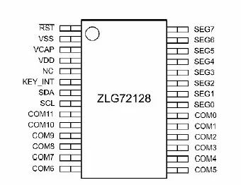
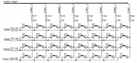
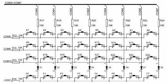
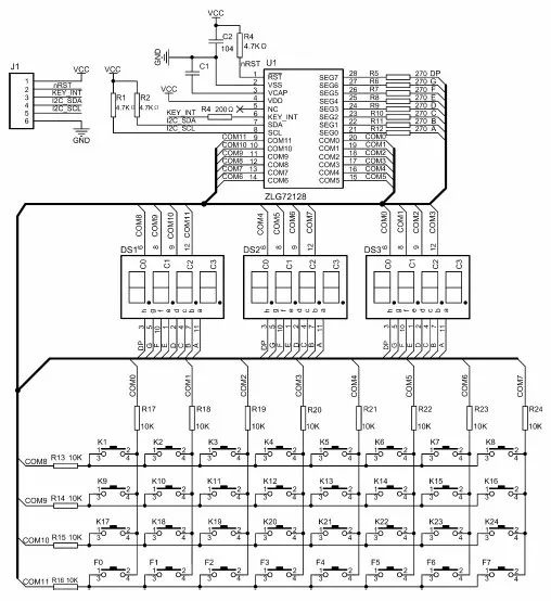
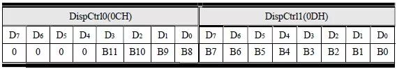
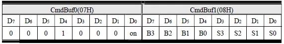
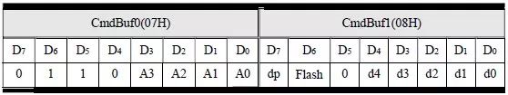
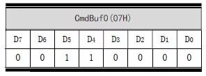
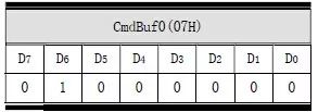
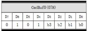
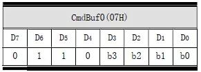
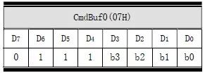
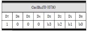
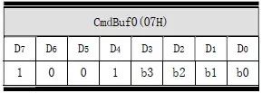
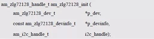
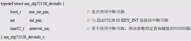
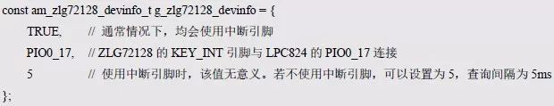
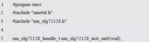
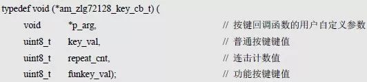
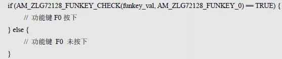
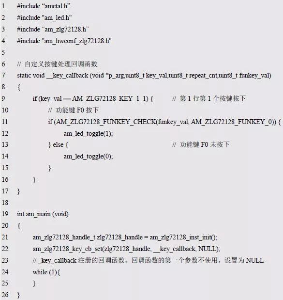
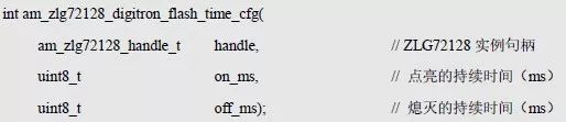
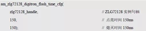
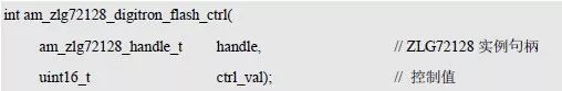
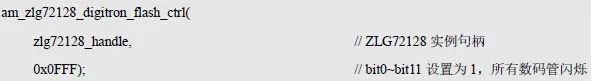
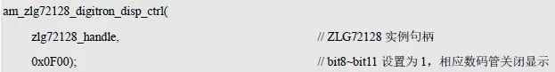
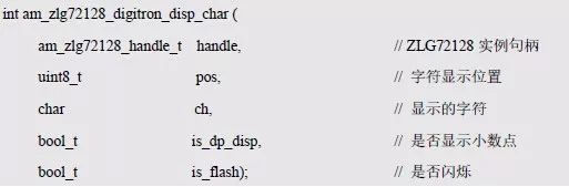
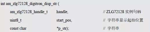
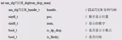
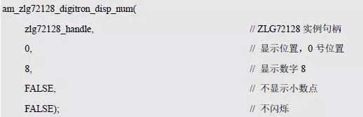
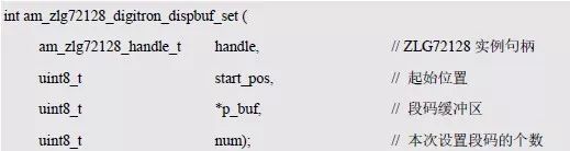
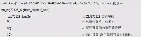
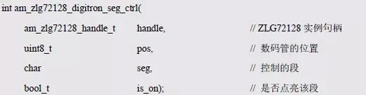
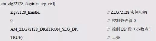
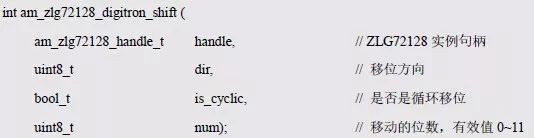
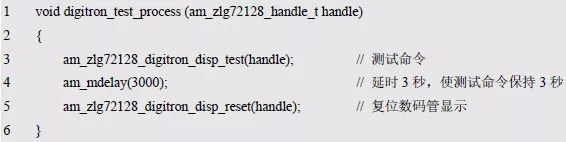
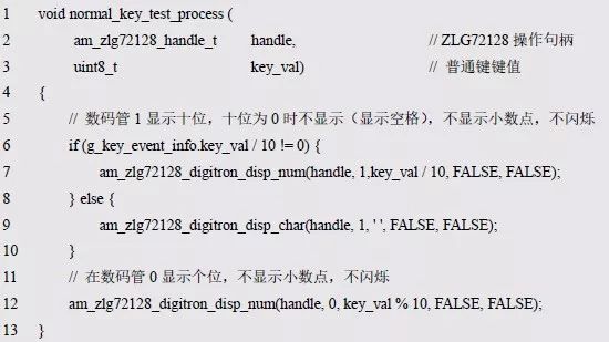
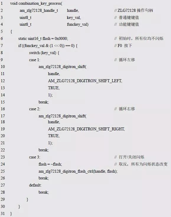
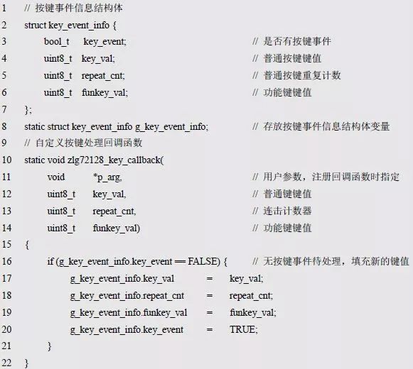
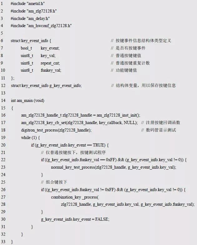
Prof. Zhou Ligong's new book "Programming for AMetal Frameworks and Interfaces (Part 1)" introduces the AMetal framework in detail. By reading this book, you can learn highly multiplexed software design principles and development ideas for interface programming. Focus on your own "core domain", change your own programming thinking, and achieve common progress between the company and the individual. The sixth chapter is to reuse the peripheral driver code . The content of this article is 6.5 keyboard and digital tube interface. 6.5 keyboard and digital tube interface > > > 6.5.1 ZLG72128 interface When the matrix is ​​expanded to a certain number, the progressive scan method is time consuming, and if it is necessary to "simultaneously" operate two or more keys, it is more troublesome to handle. ZLG72128 is ZLG's self-designed digital tube display driver and keyboard scanning management chip, which can directly drive 12-bit cascode digital tubes (or 96 independent LEDs), and can also scan up to 32 buttons, 8 of which can be scanned. Buttons can be used as function keys just like the Ctrl, Shift, and Alt keys on a computer keyboard. In addition, the ZLG72128 is also equipped with a combo counter, which enables a key to be pressed continuously without being released. The chip is an industrial grade chip with strong anti-interference ability and has been widely used in industrial measurement and control. 1. Characteristics Directly drive 12-bit, 1 inch or less common cathode digital tube or 96 independent LEDs; Ability to manage up to 32 buttons, 8 of which can be used as function keys to automatically eliminate jitter; The power circuit can easily drive large digital tubes of more than 1 inch; Powerful functions such as bit flicker, bit blanking, segment lighting, segment extinction, function keys, and combo key counting; With 10 digits and 21 letters of decoding display function, you can also directly write display data to the display buffer; Software configuration supports 0~12 digital tube display modes; An I2C serial bus interface is used with the MCU; Operating voltage range: 3.0 ~ 5.5V; Operating temperature range: -40 to +85 ° C; Package: TSSOP28. 2. Typical application circuit Figure 6.12 shows the pin arrangement diagram of ZLG72128. The corresponding pin function description is shown in Table 6.34. Table 6.34 Pin Function Table Figure 6.12 ZLG72128 pin arrangement diagram As shown in Figure 6.13, the ZLG72128 can manage up to 32 buttons (4 rows and 8 columns). The row lines are connected to COM8 ~ COM11 pins, and the column lines are connected to COM0 ~ COM7. In particular, the first 3 lines of buttons (a total of 24 buttons) are normal buttons. When the button is pressed, the user is notified via the INT pin. No notification is given when the button is released. The last row of buttons (a total of 8 buttons) is a function key that represents the state of eight key values ​​with one 8-bit data, and F0 ~ F7 correspond to bit0 to bit 7, respectively. When pressed, the corresponding bit is 0. When the corresponding bit is released, the corresponding bit is 1. As long as the 8-bit data value of the 8 buttons changes, the user will be notified through the INT pin. Therefore, for the function button, the button is pressed or released. Can be notified. Note that a resistor is required between the keyboard circuit and the ZLG72128 chip pin, which is typically 1KΩ. In most applications, you may not need so many keys, you can either cut the keyboard in rows or columns. It should be noted that this button circuit is not applicable to the case where 3 or more keys are pressed. Figure 6.13 Button circuit As shown in Figure 6.14, the button circuit is used when two or more function keys are used together with the normal keys. A diode is added between the function keys and the normal keys. Note that the diode should try to select the conduction voltage drop. smaller. Figure 6.14 Multiple function key multiplexing button circuit Figure 6.15 shows the typical application circuit schematic of the ZLG72128. When using the chip-driven digital tube and management buttons, the user can refer to the circuit for circuit design. The ZLG72128 can only directly drive a 12-bit common cathode digital tube driver. A current limiting resistor is required between the digital tube segment and the ZLG72128 chip pin. The typical value is 270Ω. If it is necessary to increase the brightness of the digital tube, the resistance value can be appropriately reduced. The driving capability of the ZLG72128 is limited. When using a large digital tube, the brightness may not be sufficient. In this case, the current limiting resistor value of the digital tube can be appropriately reduced to increase the brightness. The minimum value is 200 Ω. If the brightness is still insufficient, it must be Add the power driver circuit as described in the ZLG72128 User Manual (http://). In order to stabilize the power supply of the ZLG72128 chip, a 47~470μF electrolytic capacitor is usually connected between VCC and GND. According to the requirements of the I2C bus protocol, pull-up resistors must be connected to the signal lines SCL and SDA, respectively, which is typically 4.7KΩ. When the communication rate is greater than 100kbps, it is recommended to reduce the value of the pull-up resistor. The chip reset pin, RST, is active low and can be tied to the MCU's I/O to control its reset. The KEY_INT pin outputs a key interrupt request signal (active low) that can be connected to the MCU's I/O to get a button press or release event. Figure 6.15 ZLG72128 Typical Application Circuit 3. Register details The ZLG72128 has 12 display buffer registers, DispBuf0~DispBuf11, which directly determine what the digital tube displays. The ZLG72128 provides two display control modes, one is to write font data directly to the video memory, and the other is to automatically decode and display by writing control commands to the command buffer register. Access to these registers is done through the I2C bus interface. The I2C bus device address of the ZLG72128 is 60H (write) and 61H (read), access The internal registers are implemented by "subaddress". (1) System register SystemReg (address: 00H) The 0th bit (LSB) of the system register is called KeyAvi, which indicates whether the button is valid, 0- no button is pressed, and 1 has a button pressed. The other bits of the SystemReg register are temporarily undefined. When a key is pressed, the KEY_INT pin of the ZLG72128 generates a low interrupt request signal. When the key value is read, the interrupt signal is automatically cancelled (turns high) and KeyAvi is also reflected. Under normal circumstances, the MCU only needs to judge the KEY_INT pin. By constantly querying the KeyAvi bit, it can be judged whether there is a key press, which saves an I/O line of the microcontroller, but the I2C bus is in a frequent active state, which consumes more current and is not conducive to anti-interference. (2) Key value register Key (address: 01H) If a normal key of K1~K24 is pressed, the microcontroller can read the corresponding key value 1~24 from the key value register Key. If the microcontroller finds that the KEY_INT pin of the ZLG72128 has generated an interrupt request and the key value read from the Key is 0, it indicates that the function key was pressed. The value of the key register Key automatically becomes 0 after being read away. (3) combo counter RepeatCnt (address: 02H) The ZLG72128 provides a combo count function for K1 to K24. The so-called combo means that pressing a normal key does not let go, after a delay of two seconds, it starts to be continuous, and the continuous effective interval is about two hundred milliseconds. This feature is very similar to the keyboard on your computer. Under the premise that the microcontroller can respond to the key interrupt and read the key value in time, when pressing and holding a normal key has not been released: first, an interrupt signal will be generated, and the value of the combo counter RepeatCnt is still 0; After a two-second delay, the interrupt signal is continuously generated. Each time RepeatCent is interrupted, it is automatically incremented by one; when RepeatCnt counts to 255, it is no longer incremented, and the interrupt signal continues to be valid. During this time, the value of the key register is generated each time. (4) Function key register FunctionKey (address: 03H) The eight function keys F0 to F7 provided by the ZLG72128. Function keys are often used with normal keys, like the Shift, Ctrl, and Alt keys on a computer keyboard. Of course, the function keys can also be used separately, just like F1~F12 on the computer keyboard. When a function key is pressed, an interrupt signal is generated on the KEY_INT pin as if it were a normal key. The key values ​​of the function keys are saved in the FunctionKey register. The initial value of the function key register FunctionKey is FFH. Each bit corresponds to a function key. The 0th bit (LSB) corresponds to F0, the 1st bit corresponds to F1, and so on, and the 7th bit (MSB) corresponds to F7. When a function key is pressed, the corresponding FunctionKey bit is cleared. Another feature of the function button is the "secondary interrupt". When the button is pressed, an interrupt signal is generated. When the button is raised, an interrupt signal is generated. The normal button only generates an interrupt when it is pressed. (5) Command buffers CmdBuf0 and CmdBuf1 (addresses: 07H and 08H) The segment addressing and download display data functions can be realized by writing relevant control commands to the command buffer. (6) Flash control register FlashOnOff (address: 0BH) The FlashOnOff register determines the blink frequency and duty cycle. The reset value is 0111 0111B. The upper 4 bits indicate the duration of the flashing time, and the lower 4 digits indicate the duration of the flashing time. By changing the value of FlashOnOff, you can change the blinking frequency and duty cycle at the same time. When FlashOnOff takes the value 00H, the fastest blinking speed can be obtained. The calculation formula of the lighting off time is as follows: T = N × 50 + 150mS T is the duration of the light when it is flashing or off. N is the value of the upper 4 bits or lower 4 bits of the register, and the value is 0~15. The fastest flashing frequency is 3.33Hz (the period is 300mS), and the slowest blinking frequency is 0.55. Hz (cycle is 1.8S). Special Note: Setting the value of the FlashOnOff register separately will not see the display flicker, but should be used together with the flash control command. (7) Blanking register DispCtrl0 (address: 0CH) and DispCtrl1 (address: 0DH) As shown in Table 6.35, the blanking register is used. The DispCtrl0 and DispCtrl1 registers determine which bits are displayed, corresponding to 1 to 12 bits of the digital tube. When the register bit is 1, the corresponding digital pipe position is not displayed. The reset value is 0x00, that is, the 12 bits of the digital tube are scanned and displayed. Table 6.35 Blanking Register In practical applications, it may be necessary to display less than 12 digits. For example, only 8 digits can be displayed. In this case, the value of DispCtrl0 can be set to 0x0F, and the value of DispCtrl1 can be set to 0x00, and the 0~7 digits of the nixie tube are scanned. Display, and bits 8 to 12 are not displayed. (8) Flashing register Flash0 (address: 0EH) and Flash1 (address: 0FH) As shown in Table 6.36, the flash register is used. The Flash0 and Flash 1 registers determine which bits are blinking, corresponding to 1 to 12 bits of the digital tube. When the register bit is 1, the corresponding digital tube bit flashes. The reset value is 0x00, that is, the 12 bits of the digital tube are not flashing. Table 6.36 Flash Register In practice, some bit flicker may be needed, for example, the last 2 digits flash. In this case, the value of Flash0 can be set to 0x00, and the value of Flash1 can be set to 0x03, then the first and second digits of the nixie flash, and the third ~12 digits will not flash. (9) Display buffers DispBuf0 to DispBuf11 (address: 10H to 1BH) DispBuf0~DispBuf11 The values ​​of these 12 registers directly determine the display content of the digital tube. The 8 bits of each register correspond to the a, b, c, d, e, f, g, and dp segments of the digital tube, MSB corresponds to a, and LSB corresponds to dp. For example, the font data of the uppercase letter H is 6EH (without a decimal point) or 6FH (with a decimal point). 4. Detailed control commands The register CmdBuf0 (address: 07H) and CmdBuf1 (address: 08H) together form a command buffer. Segment addressing, downloading display data, and controlling flicker can be achieved by writing relevant control commands to the command buffer. (1) Segment addressing (SegOnOff) As shown in Table 6.37, the segment addressing register, in the segment addressing command, the 12-bit digital tube is treated as 96 segments, and each segment is actually an independent LED. Double-byte command In the instruction format, the upper 4 bits of CmdBuff0 are “0001â€, and the lowest bit of CmdBuff0 indicates whether the segment is lit, 0—off, and 1—light. B3B2B1B0 of CmdBuff0 is the bit address, which takes values ​​from 0 to 11. S3S2S1S0 is a 4-bit segment address, which takes values ​​from 0 to 7, corresponding to a, b, c, d, e, f, g, and dp of the digital tube. Table 6.37 Segment Addressing Registers (2) Download data and decode (Download) As shown in Table 6.38, the download data and decoding register, double-byte command in the instruction format, the upper 4 bits of CmdBuff0 "0010" is the command code A3A2A1A0 is the bit address of the digital tube display data, the bit address number is from left to The order of the right is 11, 10, 9, 8, ..., 0, dp controls whether the decimal point is lit, 0-off, 1-lit. Flash indicates whether to flash, 0-normal display, 1-flash. D4d3d2d1d0 is the data to be displayed, including 10 numbers and 21 letters, and the display data is decoded according to the rules in Table 6.39. Table 6.38 Download Data, Decoding Register Table 6.39 Data Table for Downloading Data and Decoding Commands (3) Reset command (Reset) Single-byte command. In the instruction format, the "4" of the upper 4 bits of CmdBuf0 is the command code. Its function is to turn off all LEDs. See Table 6.40 for details. Table 6.40 Reset Command Register (4) Test command (Test) Single-byte command. In the instruction format, the upper 4 bits of CmdBuf0 are “0100â€, which is the command code. Its function is to flash all LEDs at a rate of 0.5S. See Table 6.41 for details. Table 6.41 Test Command Register (5) Left shift command (ShiftLeft) Single-byte command. In the instruction format, the “4101†of the upper 4 bits of CmdBuf0 is the command code. See Table 6.42 for details. The function is based on the bit of the digital tube and is shifted to the left by n bits. The bit that is vacated on the right after the left shift does not display anything, that is, all LEDs are off. The value of n ranges from 1 to 11. The value greater than 11 is invalid. The value of n is determined by the lower 4 bits of CmdBuf0 and is calculated according to the following formula: n = (b3 × 8) + ( b2 × 4) + (b1 × 2) + b0 Table 6.42 Left Shift Command Register (6) Cycle left shift command (CyclicShiftLeft) Single-byte command. In the instruction format, the “0110†of the upper 4 bits of CmdBuf0 is the command code. See Table 6.43 for details. The function is based on the bit of the digital tube, and the loop is shifted to the left by n bits. After moving left, the right side shows the content removed from the far left. The value of n ranges from 1 to 11. The value greater than 11 is invalid. The value of n is determined by the lower 4 bits of CmdBuf0 and is calculated according to the following formula: n = (b3 × 8) + ( b2 × 4) + (b1 × 2) + b0 Table 6.43 Cyclic Left Shift Command Register (7) Right shift command (ShiftRight) Single-byte command. In the instruction format, the “0111†of the upper 4 bits of CmdBuf0 is the command code. See Table 6.44 for details. The function is based on the bit of the digital tube and is shifted to the right by n bits. The bit that is vacated on the left after the right shift does not display anything, that is, all LEDs are off. The value of n ranges from 1 to 11. The value greater than 11 is invalid. The value of n is determined by the lower 4 bits of CmdBuf0 and is calculated according to the following formula: n = (b3 × 8) + ( b2 × 4) + (b1 × 2) + b0 Table 6.44 Right Shift Command Register (8) Cycle right shift command (CyclicShiftRight) Single-byte command, in the instruction format, the "1000" of the upper 4 bits of CmdBuf0 is the command code. See Table 6.45 for details. The function is based on the bit of the digital tube, and the loop is shifted to the right by n bits. After shifting right, the left side shows the content shifted from the rightmost side. The value of n ranges from 1 to 11. The value greater than 11 is invalid. The value of n is determined by the lower 4 bits of CmdBuf0, and is calculated according to the following formula: n = (b3 × 8) + ( b2 × 4) + (b1 × 2) + b0 Table 6.45 Loop Right Shift Command Register (9) Digital tube scanning digit setting command (Scanning) For single-byte commands, the "4" of the upper 4 bits of CmdBuf0 in the instruction format is the command code, and the number of bits scanned by the digital tube is set. See Table 6.46 for details. The value of n is 0~12, which is greater than 12 and is scanned by 12 bits. The number of scan bits n is valid from the first bit of the bit select to the nth bit of the bit select. The value of n is determined by the lower four bits of CmdBuf0 and is calculated according to the following formula. n = (b3 × 8) + ( b2 × 4) + (b1 × 2) + b0 Table 6.46 Scan Digits Setting Register During use, if a 12-digit display is not required, crop from the highest position and set the number of digital scan bits to the corresponding number of digits. After the number of scan bits of the digital tube is reduced, the useful display position is increased due to the more scan time allocated. > > > 6.5.2 ZLG72128 Initialization AMetal has provided the ZLG72128 driver function. Before using other functions to manage the digital tube and buttons, the ZLG72128 must be initialized. The prototype of its initialization function (am_zlg72128.h) is: This function is intended to get the instance handle of ZLG72128. Where p_dev is a pointer to an instance of type am_zlg72128_dev_t and p_devinfo is a pointer to instance information of type am_zlg72128_devinfo_t. Instance The definition of the am_zlg72128_dev_t type (am_zlg72128.h) is as follows: Where g_zlg72128_dev is a user-defined instance whose address is passed as an argument to p_dev. Instance information The instance information describes the information about the interrupt pin. The definition of the type am_zlg72128_devinfo_t (am_zlg72128.h) is as follows: Where use_int_pin indicates whether to use the interrupt output pin (KEY_INT) of the ZLG72128. If the value is TRUE, it indicates that the interrupt pin needs to be used. At this time, int_pin specifies the pin number connected to the main controller (such as LPC824). The key value will be obtained in the pin interrupt; if the value is FALSE, it means no The interrupt pin is used, at which time interval_ms specifies the time interval for querying the key value. In general, the interrupt pin is used as long as the I/O resources of the master are not very tight. To save an I/O interrupt resource, use_int_pin can be set to FALSE. At this time, the IO interrupt resource will not be occupied, and the system will get the key value from the ZLG72128 by query, which will consume a certain amount of CPU resources. Because every time you have to actively query the key value. Assuming the interrupt pin of the ZLG72128 is used, the host controller uses the LPC824, and the KEY_INT pin of the ZLG72128 is connected to the PIO0_17 of the LPC824. Its instance information is defined as follows: I2C handle i2c_handle If the I2C1 of the LPC824 is used to communicate with the ZLG72128, the I2C handle can be obtained by the I2C1 instance initialization function am_lpc82x_i2c1_inst_init() of the LPC82x. which is: The obtained I2C handle can be passed directly as an argument to i2c_handle. Example handle The return value of the am_zlg72128_init() function is the handle of the ZLG72128 instance, which will be used as the argument to the first parameter (handle) of other functional interfaces (digital tube display, button management, etc.). Its type am_zlg72128_handle_t(am_zlg72128.h) is defined as follows: If the return value is NULL, the initialization fails; if the return value is not NULL, a valid handle is returned. Based on the modular programming idea, the definitions of the initialization related instances, instance information, etc. are stored in the corresponding configuration file, and the instance initialization function interface is extracted through the header file. The program examples of the source file and the header file are respectively shown in the program list 6.111 and the program. Listing 6.112. Listing 6.111 ZLG72128 Instance Initialization Function Implementation (am_hwconf_zlg72128.c) Listing 6.112 ZLG72128 Instance Initialization Function Declaration (am_hwconf_zlg72128.h) Subsequent only need to use the parameterless instance initialization function to get the instance handle of ZLG72128. which is: > > > 6.5.3 Button management interface function The ZLG72128 supports 32 keys (4 rows and 8 columns matrix keyboard), where the first 3 acts as a normal key, and only one normal key can be pressed at a time. The last action function key, multiple function keys can be pressed simultaneously. The button management has only one registration button callback interface function. In order to notify the user of the key event in time when the key event is detected (the key is pressed), the user needs to register a callback function, and when a key event occurs, the user registered callback function is automatically invoked. Its function prototype is: Among them, pfn_key_cb is the registered key callback function, p_arg is the value of the first parameter of the callback function, that is, when the callback function is automatically called when the key event is detected, the value of p_arg is used as the value of the first parameter of the callback function. The type of callback function am_zlg72128_key_cb_t(am_zlg72128.h) is defined as follows: It can be seen that the callback function has 4 parameters, and the user can obtain the information related to the button through these parameters. In particular, the first parameter p_arg is a user-defined parameter whose value is the value set by the p_arg parameter when registering the callback function. Key_val, repeat_cnt, and funo_val represent information about key events. There are three possible key events for ZLG72128: There is a normal button press (normal button release does not act as a button event) When a normal key is pressed, key_val indicates the key value of the pressed key. The valid range of the key value is 1 ~ 24, and the key value of the normal key has been defined as a macro in am_zlg72128.h, and the macro name is AM_ZLG72128_KEY_X_Y, where X represents Line number (1 ~ 3), Y means column number (1 ~ 8), such as the key value of the 5th key of the 2nd line: AM_ZLG72128_KEY_2_5. The normal button is pressed all the time (in the combo state) When the normal key presses for more than 2 seconds, it enters the combo state. When it is in the combo state, a button event is generated every 200ms, and a button counter is used to count the generated button events. Each button event is generated. The value of the counter is incremented by 1. Since the bit width of the combo counter is 8 bits, the value will not be incremented after the value reaches 255, but the button event will continue to be generated until the key is released and the combo counter is cleared. In the combo state, key_val indicates the key value of the pressed key, and repeat_cnt indicates the value of the combo counter. The status of the function key changes (the function key is pressed or released, causing the status to change) The value of funkey_val represents the state of all function keys. The last line has up to 8 keys, from left to right, respectively F0 ~ F7, one-to-one correspondence with bit0~bit7 of funkey_val. A bit value of 0 means that the corresponding function key is pressed, and a bit value of 1 means that the corresponding function key is not pressed. When no function key is pressed, the value of funkey_val is 0xFF. As long as the value of funkey_val changes, a button event is generated and the function key does not provide a combo function. You can use macros in am_zlg72128.h AM_ZLG72128_FUNKEY_CHECK(funkey_val, funkey_num) to easily determine whether a function key is pressed. Funkey_num is used to indicate the function key to be detected. The value has been defined as a macro. F0 ~ F7 are AM_ZLG72128_FUNKEY_0 ~ AM_ZLG72128_FUNKEY_7 respectively. If the corresponding key is pressed, the macro value is TURE; otherwise, the macro value is FALSE. For example, if you know if F0 is pressed by funkey_val, you can use the following statement: The function keys are similar to the Ctrl, Alt, Shift keys on the PC. It is easy to implement the combination key using the normal keys and function keys. The sample program for registering the key callback function is shown in Listing 6.113. Listing 6.113 ZLG72128 Registration Key Callback Function Usage Example If only the first key of the first line is pressed, the LED0 state is reversed. If the first key of the first row is pressed and the function key F0 is pressed, the LED1 state is reversed. This example simply shows the combination. How to use the key. > > > 6.5.4 Digital tube display interface function ZLG72128 supports 12-bit cascode digital tube, as well as flicker, displacement and other functions. Although there are many kinds of interface functions, the functions of each interface function are relatively simple. The following describes the use of each interface function. 1. Flashing duration When the nixie is flashing, the function prototype for setting its duration of illumination and extinction is: At power-on, the default duration of the digital tube on and off is 500ms. The valid time values ​​for on_ms and off_ms are 150, 200, 250, ..., 800, 850, 900, ie 150ms ~ 900ms, and the time interval is 50ms. If the time interval is not these values, you should choose the closest value. For example, set the digital tube to flash at the fastest frequency, that is, the minimum time for light and off is 150ms. The usage method is as follows: Note: Only setting the flashing time can not immediately see the flicker phenomenon, you must turn on the flashing switch of a certain bit to see the flicker phenomenon. See the am_zlg72128_digitron_flash_ctrl() function for details. 2. Flicker control The function prototype that controls whether the digital tube is blinking is: Among them, ctrl_val is the control value, bit0 ~ bit11 are valid bits, corresponding to the digital tube 0 ~ 11, respectively, the bit value is 0, it does not flash, and when the bit value is 1, it flashes. The default value of power-on is 0x0000, that is, all digital tubes are not flashing. For example, to control the flashing of all digital tubes, the method of use is as follows: Note: Since the digital tube may not display anything at the beginning, this code may not see flicker, so you can use the subsequent related APIs to display the digital tube with some actual and effective content before setting. 3. Display properties (on or off) The display attribute refers to which digital tubes are displayed and which digital tubes are not displayed. By default, all digital tubes are turned on and the 12-digit digital tube is scanned. In fact, you may need to display fewer than 12 digits. You can use this function to turn off the display of certain bits. Its function prototype is: Among them, ctrl_val is the control value, bit0 ~ bit11 are valid bits, respectively corresponding to the digital tube 0 ~ 11, the bit value is 0, the display is turned on, and when the bit value is 1, the display is turned off. The default value of power-on is 0x0000, that is, all bits are displayed normally. For example, only the digital tube 0 ~ 7, using this, you can turn off the digital tube 8 ~ 11, its use is as follows: Note: When using this function to control the display properties, the segment code content of the corresponding digital tube will not change. 4. Display character Displaying characters at the specified position, ZLG72128 has provided 10 digits of 0 ~ 9 and the common 21-letter automatic decoding display, no need to apply and then self-decode. Its function prototype is: The characters displayed must be characters that ZLG72128 has supported to auto-decode, including the characters '0' to '9' and AbCdEFGHiJLopqrtUychT (case sensitive). Note that to display the number 1, the ch parameter should be the character '1' instead of the number 1. Returns -AM_ENOTSUP if the specified character is not supported. Returns AM_OK as long as it is displayed successfully. If you need to display some custom graphics, use am_zlg72128_digitron_dispbuf_set() to directly set the displayed segment code. For example, if the character F is displayed in the digital tube 0, the decimal point is not displayed, and no flashing is used. The usage is as follows: 5. Display string Specify the starting position of the string display and start displaying a string. Its function prototype is: The string display encounters the character end flag '\0' will end automatically, or will automatically end when the valid character display area is exceeded. The characters displayed should be guaranteed to be automatically decoded by the ZLG72128, including the characters '0' to '9' and AbCdEFGHiJLopqrtUychT (case sensitive). If there are characters that are not supported, the corresponding location will not display anything. For example, starting with the digital tube 0, the string "0123456789" is displayed, which is used as follows: 6. Display numbers from 0 to 9 Display the number from 0 to 9 at the specified position. The function prototype is: This function is only used to display a number from 0 to 9. If the number is greater than 9, each bit should be displayed separately as needed. Note that the num parameter is the number 0~9, not the characters '0'~'9'. For example, the digital tube 0 displays the number 8, does not display the decimal point, does not flash. Its use is as follows: 7. Directly set the digital tube display segment code This function is used to set the segment code displayed by each digital tube. When you need to display some graphics or characters that cannot be automatically decoded, you can use this function to flexibly display various graphics. Its function prototype is: This function can set the buffer contents displayed by multiple consecutive digital tubes at a time. The initial display position is specified by start_pos, and the effective value is 0 ~ 11. The number of consecutively displayed digital tubes is specified by the parameter num. This function will set the display contents of each digital tube of start_pos~ (start_pos + num -1) in order. The segment code is 8 bits, and bit0~bit7 correspond to segments a ~ dp respectively. When the bit value is 1, the corresponding segment is lit. When the bit value is 0, the corresponding segment is off. If the number 1 is displayed, the segment b and the segment c need to be illuminated. This requires bit1 and bit2 to be 1, so the segment code is 00000110, which is 0x06. Other display graphics can be deduced by analogy. For example, in the digital tube 0 ~ 9 display the number 0 ~ 9, you can use this function to directly set the segment code displayed by each digital tube, the use is as follows: 8. Direct control of the segment is lit or extinguished Although a function for directly setting the display segment code has been provided, in order to display a graphic more flexibly, or to control the transformation of the graphic. The ZLG72128 supports direct control of the on and off of a segment. Its function prototype is: Pos is used to specify the position of the digital tube. Valid values ​​are 0~11. Seg indicates the segment to be controlled. The valid values ​​are 0~7, corresponding to a ~ dp. The sections have been defined in the form of macros in the am_zlg72128.h file. It is not recommended to use the immediate 0~7 directly. Instead, use the macro AM_ZLG72128_DIGITRON_SEG_A ~AM_ZLG72128_DIGITRON_SEG_DP corresponding to a ~ dp. For example, on the basis of the current display, you need to display the decimal point in the digital tube 0, and the other contents are unchanged. At this time, you can directly use this function to control the dp segment of the digital tube 0. The usage is as follows: Note: Only one segment can be controlled at a time. 9. Display shift control The ZLG72128 supports shift control, which allows all digital tubes to be shifted according to commands. A total of 4 shift modes are supported, left shift, loop left shift, right shift, and loop right shift. Its function prototype is: Dir specifies the shift direction. The macro value indicating the direction has been defined in the am_zlg72128.h file using the form of the macro. The macro value should be used directly as the value of the dir parameter, left to AM_ZLG72128_DIGITRON_SHIFT_LEFT and right to AM_ZLG72128_DIGITRON_SHIFT_RIGHT. When is_cyclic is TRUE, it indicates that it is a cyclic shift, otherwise it is not a cyclic shift. If it is not a cyclic shift, after the shift, the bit that is vacated on the right (shifted to the left) or the bit that is vacated on the left (shifted to the right) will not display anything. If it is a loop move, the vacated bit will show the contents of the removed bit. Num specifies the number of bits to move, which can be moved from 0 to 11 bits at a time. Values ​​greater than 11 are treated as invalid values. For example, to shift the current digital tube display to the left by one bit, the usage is as follows: In practice, you may find that the shift direction is exactly the opposite of the incoming command, which is due to the difference in hardware design. Commonly, there are two possible hardware design methods: The far right is the digital tube 0, from left to right: 11, 10, 9, 8, 7, 6, 5, 4, 3, 2, 1, 0 The leftmost digit is the digital tube 0, from left to right: 0, 1, 2, 3, 4, 5, 6, 7, 8, 9, 10, 11 This mainly depends on the physical location of the digital tube corresponding to the COM0 ~ COM11 pin during hardware design. The concept of left shift and right shift here is based on the ZLG72128 typical application circuit, and COM0 corresponds to the rightmost digital tube, that is, the rightmost digit is the digital tube 0. Then the concepts of left and right shift are: Left shift: The digital tube 0 (the rightmost digital tube) display switches to 1, the digital tube 1 display switches to 2, ..., and the digital tube 10 display switches to 11. Right shift: The digital tube 11 (leftmost digital tube) display switches to 10, the digital tube 1 display switches to 2, ..., and the digital tube 10 display switches to 11. If the hardware circuit design digital tube position is reversed (such as COM0 corresponds to the leftmost digital tube), the shift effect is exactly the opposite, so only a little attention is needed here. 10. Reset display The reset display clears the contents displayed by the digital tube, that is, all digital tubes do not display anything. Its function prototype is: 11. Test command The test command is mainly used to test whether the hardware circuit of the digital tube is connected properly. Its function prototype is: After executing the test command, the digital pipe segment displays “8.8.8.8.8.8.8.8.8.8.8.8.†and flashes at a rate of 0.5 s. 12. Digital tube display test In order to judge whether the digital tube is working properly, a simple digital tube display test is realized: when the system is started, the digital tube enters the test state, and all the segments of the digital tube are illuminated, that is, “8.8.8.8.8.8.8.8.8.8.8.8. ", and flashes at a rate of 0.5s. After 3 seconds, the display is cleared. Because the ZLG72128 comes with a digital tube test command, this function is very easy to implement, directly call the test command interface, after a delay of 3s, reset the digital tube display. The sample program is detailed in Listing 6.114. Listing 6.114 Digital Tube Display Test Sample Program 13. Single normal key test To test whether each of the normal keys is working properly, implement a simple button test: press any of the normal keys, the digital tube displays the key value of the current key (1~24). For ordinary keys, when the key is pressed, the key value (1~24) can be directly obtained through the key callback function. After the key value is obtained, the value can be displayed by using the digital tube display interface. The sample program is detailed in Listing 6.115. Listing 6.115 General Key Test Sample Program 14. Combination key use The ZLG72128 has 8 function keys. The function keys are like the Ctrl, Shift and Alt keys of the computer keyboard. Combined with other common keys, you can implement rich functions such as Ctrl+S (save), Ctrl+A (select all), Ctrl+Z. (revoked) and so on. Here, the function key F0 is taken as an example to show how it can be combined with a normal button. For the convenience of observation, define the following operations and corresponding phenomena: F0 + K1: The digital tube display cycle left shift; F0 + K2: The digital tube display is rotated to the right; F0 + K3: All flashing displays are turned on/off. The functions corresponding to the various key combinations have corresponding APIs. The corresponding sample programs are detailed in Listing 6.116. Listing 6.116 Key Combination Using the Sample Program At this point, the processing functions of each function are written. But for the handling of key events, there is a key step to get the key value. Through the introduction of the ZLG72128 interface function, if you need to get the key value, you only need to register the key callback function, and then you can get the key value in the callback function through the parameters passed to the callback function. According to conventional thinking, after obtaining the key value, it is possible to call the relevant processing function directly in the callback function to process the button accordingly, but this is very inappropriate. This is because the callback function is generally executed in the interrupt environment. If the processing of the callback function takes a long time, it will seriously affect the real-time performance of the entire system. It should be guaranteed that the processing of the callback function ends as quickly as possible. Based on this, only the key value is saved in the key callback function, and the actual processing is completed in the main loop of the am_main() function. Therefore, the processing of the callback function is very simple, just save the key value and set a flag for the main loop query of am_main(). The sample program is detailed in Listing 6.117. Listing 6.117 Callback Function Processing Sample Program Here, a key event information structure variable is defined, and all relevant information in the key callback function is stored in the structure. When the value of key_event is TRUE, there is a button event. The sample program is shown in Listing 6.118. Listing 6.118 Synthesis Sample Program Usually, there are certain restrictions on smart portable projectors in 2 aspects: smart portable projector,smart portable projector for iphone,best smart portable projector 2020,cheap smart portable projector,mini smart portable projector wifi Shenzhen Happybate Trading Co.,LTD , https://www.szhappybateprojectors.com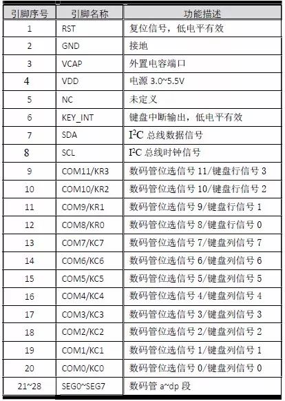


1. Size: Usually the size is the size of a mobile phone.
2. Battery life: It is required to have at least 1-2 hours or more of battery life without power connection. In addition, its general weight will not exceed 0.2Kg, and some do not even need fan cooling or ultra-small silent fan cooling. Can be carried with you (it can be put into a pocket, the screen can be projected to 40-50 inches or more, so sometimes we also call it a pico projector or a pocket projector.)