Design of LED drive power PFC circuit
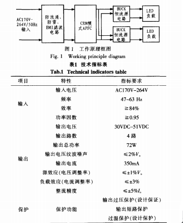
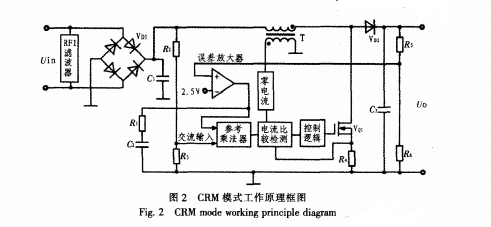
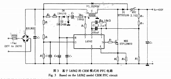
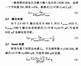
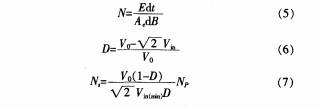
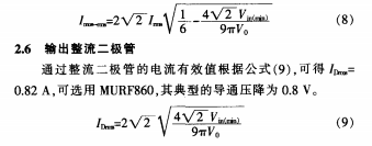
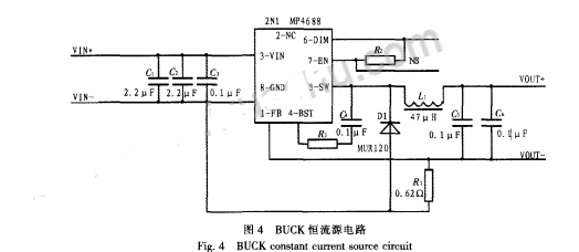
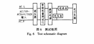
The LED driving power supply is a power converter that converts the power supply into a specific voltage and current to drive the LED to emit light. Generally, the input of the LED driving power source includes high-voltage power frequency alternating current (ie, commercial power), low-voltage direct current, high-voltage direct current, low voltage high. Frequency communication (such as the output of an electronic transformer). The output of the LED driver is mostly a constant current source that changes the voltage as the LED's forward voltage drop changes. 1.1 Working principle LED drivers are primarily used for high power lighting. The design must meet the normal lighting requirements; meet the high efficiency, low cost and small size; the output of the power driver must be controlled by constant current; fully consider the safe work. The AC input first enters the lightning protection and EMI road. This part of the circuit prevents external interference from entering the power supply, and prevents internal interference from entering the AC transmission system. The normal input AC is rectified and filtered, and enters the power factor correction circuit. Perform voltage and current waveform modulation to achieve power factor and current harmonic requirements; achieve constant current output through constant current control circuit to achieve normal LED operation. Working principle diagram, as shown in Figure 1. 1.2 Technical indicators System design technical requirements, as shown in Table 1. The system is cheap to use, easy to design, and has no turn-on loss. When the booster tube is turned off, the zero current is naturally turned off, and the peaks are small. The critical conduction type control mode (CRM) with the corresponding loss is also small, and the working principle block diagram of the CRM mode is shown in Fig. 2 [6-8]. There are many chips for CRM mode control. ST's L6562D chip has the characteristics of excellent performance, high reliability, low price, etc., so the chip is selected. The system uses the control chip L6562D to design the PFC circuit. It has a simple external circuit, current limit one by one pulse, programmable output overvoltage protection and open loop protection. The circuit principle is shown in Figure 3. 2.1 high frequency filter capacitor The minimum design, minimum input voltage and maximum output power are V(nln)=17V, V(唧)=264V, Po)=90W, PFC circuit operating frequency f~=90kHz, output voltage Vo=400V, PFC circuit efficiency 7/=96%, according to formula (1) can get Im=O. 58A. 2.4 Transformer turns Therefore, the inductor is used not only as an inductor but also as a transformer to generate the power required to control the IC. It can be calculated that the operating frequency is 170VAC when the input voltage is used. As the secondary side of the transformer, it must be ensured that the IC can work normally. The operating voltage is set to 18V. Select TDK's PQ26/2o core: Ae=l19mm. Take the largest magnetic flux density: AB = O. 25T. According to formula (5), Nr. =49.5, choose 50åŒ. According to formula (6), D = 0.4 can be calculated. According to formula (7), Ns = 5 å¯ can be obtained. The primary current of the 2.5PFC MOSFET is the maximum at the lowest voltage, which is calculated by the approximation of equation (8). 0.58A, in fact, when the MOSFET is turned off, there is no current flowing on it, and the FET SPP20-N60C3 can be selected. 3.1 protection function The system design requires protection functions such as overvoltage, short circuit and overtemperature of the output. VIN0=2.2uF. L_FC3=0.1uF Output overvoltage protection is by detecting the output voltage when the output voltage exceeds the protection point. The trigger signal is transmitted to the primary through the light disaster isolation, and the COMP terminal of the control chip L6565D is pulled down, so that the power supply has no output. Output short circuit protection is to sample the output current through the resistor. When the output current exceeds the set protection point (2A), the comparator flips and the drive light is turned on. The secondary of the light fault will control the COMP end of the chip L6565D, so that the power supply has no output. When the short-circuit state is released, the output can be automatically restored. The output over-temperature protection is realized by connecting a 105°C normally-closed temperature relay ST-22 in series with the power supply terminal VCC of the control chip L6565D. The temperature relay is mounted on the heat sink of the main power tube. When the temperature exceeds 105oC, the temperature relay is turned off, the power output is turned off, and when the temperature returns to about 95 °C, the temperature relay is reclosed. The power output is restored. 3.2BUCK constant current source circuit The BUCK circuit has a simple topology, few external components, and high efficiency. The circuit principle is shown in the figure. The control chip selects MP4688 of MPs, and the circuit is shown in Figure 4. 3.3 anti-surge, lightning protection, EMI filter circuit This power supply is for LED street lights. Anti-surge and lightning protection are basic requirements First, the large input power (about 90W) makes EMI filtering also an important indicator requirement. For these three technical indicators, the design circuit is shown in Figure 5. Varistor RV. To prevent surge, RV:, RV3, VG1 (gas discharge pipe) together constitute a lightning protection circuit, common mode inductance, L. cI-C constitutes an EMI filter circuit, fuse F1 provides input short-circuit protection, and ~3 is C. Provide a discharge path. 4 system test test block diagram shown in Figure 6. A4.1 Insulation resistance test The insulation voltage tester is used to test the input and output of the tested power supply. The insulation resistance Ra of the input and output to the outer casing should be greater than or equal to 50MI}. The test voltage is DC500V, and the input terminal and output terminal are shorted respectively. 4.2 Insulation strength test Use the insulation withstand voltage tester to test the power supply under test. The following conditions shall be applied and kept for 1 min, and there shall be no breakdown or flashover. Shorten the input terminal and output terminal separately. 4.3 Short-circuit protection function test Connect the power supply, voltage regulator, intelligent power meter, measured power supply, electronic load and various measuring instruments according to the test block diagram. Adjust the voltage regulator to make the input voltage AC230V. The power supply under test works normally. The short circuit function of the electronic load is used to short-circuit the output of the power supply under test, and then the short-circuit state is released, and the power supply under test should be able to resume normal operation. The short-circuit protection function of the tested power supply is normal. 4.4 high and low temperature work test Put the power supply under test into the temperature test chamber, and connect the instrument and electronic load according to the test block diagram. Start the temperature test chamber to cool to a temperature of 45 ° C ± 2 ° C. After 2 hours of constant temperature, power up and test. The temperature rises after the test is completed. During the heating process, the rated working state of the tested power supply is maintained, the temperature is raised to +45oC±2oC, and the test is performed after the constant temperature is applied for 2 hours. Through the test, the solution of the system is effective, the efficiency of the converter is improved, and the overall efficiency of the power source meets the technical requirements. From the experimental data results and waveforms, it is concluded that the LED driver power supply based on PFC design and implementation is reasonable in design, reliable and stable in debugging and testing, and performance and indicators meet the design requirements. LED is considered to be the most promising lighting source in the future, and LED driver power is the most important factor affecting and restricting LED life. This paper is based on this prospect, developed PFC-based LED drive power. The drive power loss is low, with high power factor and efficiency. The driving power circuit has a simple form, few external components, small volume, high power density, high reliability, good waterproof and dustproof effects, and all performances meet the standard requirements.
Problems with failing factory relays, connectors/terminals and fuse contacts are also common when excessive load is placed on them.
Yacenter
has experienced QC to check the products in each process, from developing
samples to bulk, to make sure the best quality of goods. Timely communication
with customers is so important during our cooperation.
If you can't find the exact product you
need in
the pictures,please don't go away.Just contact me freely or send your sample
and drawing to us.We will reply you as soon as possible.
Plate Harness,Pcb Board Harness,Pcb Board Wiring Harness,Pcb Plate Harness Dongguan YAC Electric Co,. LTD. , https://www.yacentercns.com