Designing FPGA-based high-speed data acquisition system with AD574A
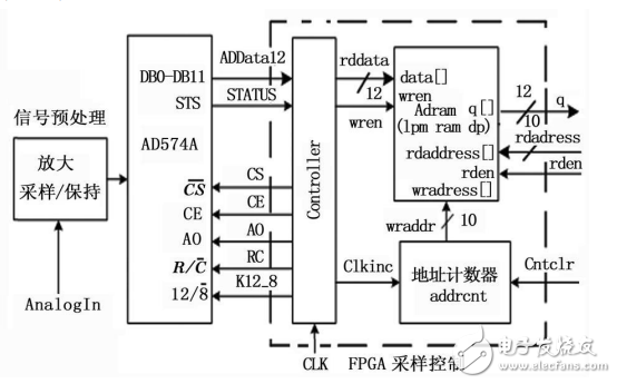
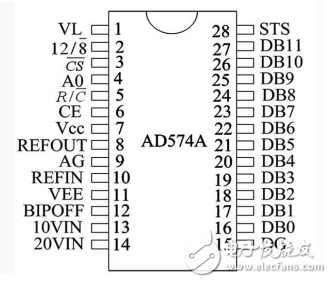
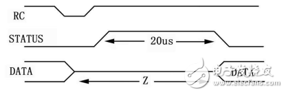
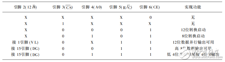
In the automatic control and detection system, the acquisition and processing of analog signals are often involved. The general practice is to use the microcontroller and other chips to expand the system resources to achieve the desired functions, but this will make the external circuit scale and system cost significant. The increase, which leads to the complexity of the system design, is generally difficult to achieve higher sampling speed. Designing a high-speed sampling control system based on FPGA is flexible and convenient, which can greatly improve the overall performance of the system. The structure and working principle of the data acquisition control system designed in this paper is shown in Figure 1. The system consists of the FPGA sampling control module to form the core circuit of the system. The module is mainly composed of three parts: controller (Controller), embedded dual-port RAM (Adram), and address counter (Addrcnt). The system works as follows: The controller (Controller) controls the AD574A and writes to the Adram. The address counter (Addrcnt) acts in two cases: (1) when the clear terminal Cntclr of the counter is high, its output is 0; (2) when the rising edge of the clock Clkclr comes, it starts counting and provides storage. The address saves the collected data. The embedded dual-port RAM (Adram) is used to implement the RAM in the FPGA to store the acquired data. At the same time, external devices (such as DSP, MCU, etc.) can read in the data for further processing. When wren is at a high level, the acquired data can be saved in the corresponding memory location according to the input address. As a fast 12-bit successive comparison A/D converter chip with a three-state buffer, the AD574A can be directly connected to an 8-bit or 16-bit microprocessor without the need for additional logic interface circuitry. The chip has a clock source and a reference voltage source, and it does not need an external clock and reference voltage to operate normally. The AD574A has a conversion time of 25μs and a linearity error of ±1/2LSB. The chip contains successive STS approximation register SAR, DAC conversion circuit, control logic, comparator and tristate buffer. Single channel unipolar or bipolar voltage input and 28-pin dual vertical plug-in package. The AD574A consists of a 12-bit A/D converter, control logic, a three-state output latch buffer, and a 10V reference. The chip has two modes of operation: a single operating mode and a full-speed operating mode (Figure 1). Figure 1 Principle structure of the data acquisition control system The AD574A is packaged in dual in-line mode with 28 pins (Figure 2), where CS is the chip select signal and active low; CE is the chip enable signal, active high; only CS and CE are active at the same time The AD574A can work. R/C is a read or switch control signal that controls whether ADC 574A is a conversion or a read. When it is low, A/D conversion is started; when it is high, the conversion result is read. 12/8 is the data output mode control signal. When it is high level, the output data is 12 bits; when it is low level, the data is output as two 8-bit words. A0 converts the bit number control signal. When it is high level, it performs 8-bit conversion, and when it is low level, it performs 12-bit conversion. The operation functions are shown in Table 1, and the corresponding operation timing diagram is shown in Figure 3. Figure 2 pin diagram Figure 3 working sequence diagram Table 1 AD574A Operation Function Table for Different Pin State Combinations Array Speakers,Waterproof Loudspeaker,Line Array Speaker,Linear Array Loudspeaker NINGBO SANCO ELECTRONICS CO., LTD. , https://www.sancobuzzer.com