Application of Silicon Spread Spectrum Oscillator in Automotive Electronics
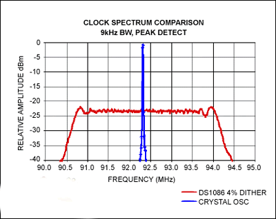
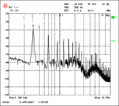
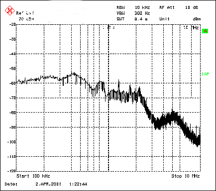
Advantages of Spread Spectrum Oscillator in Automotive Electronics Design This article refers to the address: http:// Spread spectrum technology can well meet FCC specifications and EMI compatibility requirements, and EMI compatibility depends to a large extent on the passband specifications of measurement technology. The spread-spectrum oscillator fundamentally solves the problem of high concentration of peak energy, which is distributed in the noise floor, which reduces the system's need for filtering and shielding, and brings other benefits. High-quality multimedia, audio, video, and wireless systems are gaining more and more of today's automotive electronics, and designers have to consider the radio frequency (RF) energy that is distributed across the sensitive frequency bands of these subsystems. For high-quality wireless devices, the ability to eliminate RF peak energy directly determines the effectiveness of the solution. For many years, wireless communication products have used "frequency adjustment" techniques to avoid the effects of power switching noise. Such wireless devices are capable of communicating with a power supply such that the power supply changes its switching frequency as commanded, moving the energy peak beyond the tuner input frequency band. In modern automotive electronics, as the number of interference sources increases, it is difficult to ensure that the systems work together. This situation is complicated by the variety of equipment antennas and the restrictions on the placement of newly added subsystems. Spread-spectrum oscillators have unique advantages in systems such as digital audio, factory assembly, hands-free devices, etc. These systems typically use codecs to improve audio quality, and codecs are connected to cellular phones or other information processing terminals via digital interfaces. If a "jitter" (spread spectrum) oscillator is used as the clock source for the codec, harmonic noise can be eliminated in a non-silent condition. This technique is common in multimedia systems that use switched capacitor codecs. In addition to suppressing harmonic noise, the SS oscillator is capable of reducing the energy peak to within the noise floor, and reduces interference that falls within the channel in a wireless frequency hopping network. In the next generation of automotive electronics, almost all subsystems tend to use SS clock technology to improve system performance and reduce EMI. For this application, Maxim/Dallas has introduced an all-silicon oscillator that is reliably oscillating and shock-resistant. Its cost is very competitive with ceramic resonators, with oscillation frequencies ranging from a few kilohertz to tens of megahertz. Automotive electronics design considerations Effective control of EMI is a key issue for electronics engineers in product design. Digital system clocks are an important source of EMI. The main reason is that clocks generally have the highest frequency in the system, and are often periodic square waves, clocks. The lead length is usually the longest in system wiring. The spectrum of the clock signal includes the fundamental and harmonics, and the amplitude of the harmonic components decreases as the frequency increases. Other signals in the system (signals on the data or address bus) are refreshed at a frequency synchronized with the clock, but the data refresh actions occur at uncertain time intervals and are not related to each other. The resulting noise spectrum occupies a wide frequency band, and the noise amplitude is much lower than the noise amplitude generated by the clock. Although the total noise energy produced by these signals is much higher than the clock noise energy, it has very little impact on EMI testing. The EMI test focuses on the magnitude of the highest spectral power density, not the total radiant energy. In practical applications, EMI can be improved by filtering, shielding, and good PC board layout. However, adding filters and shielding increases the cost of the system, and accurate board layout takes a long time. Another way to solve the EMI problem is to start directly from the noise source (usually the clock oscillator), and the clock frequency that changes over time can easily reduce the fundamental and harmonic amplitude. The energy of the clock signal is constant, and the clock of varying frequency broadens the spectrum, thus reducing the energy of each harmonic component. A simple way to generate such a clock is to modulate a voltage controlled oscillator (VCO) with a triangular wave, and the resulting clock spectrum range increases as the amplitude of the triangular wave increases. In practical applications, it is necessary to reasonably select the repetition period of the triangular wave. When the frequency of the triangular wave is low, the coupling noise is generated by the power supply to the analog subsystem; if the frequency is too high, the triangular circuit will interfere with the digital circuit. Figure 1 is a schematic diagram of a clock oscillator based on the above considerations. It uses a triangular wave to control the bandwidth of the VCO output spectrum. The center frequency of the VCO is controlled by a DAC and a programmable 8-bit divider, which can set the frequency from 260kHz to 133MHz. The IC shown in Figure 1 is controlled by a 2-wire interface. The control word is stored in the EEPROM inside the chip. If the frequency is set to the desired frequency in advance, the device can work in stand-alone mode or update the frequency during its idle period. This is also an advantage in low power applications. Figure 1 The core circuit of the DS1086 programmable clock generator is a triangular-controlled VCO. The frequency is programmed through a 2-wire interface and stored in the on-chip EEPROM. Figure 2 shows a spectrum comparison of a normal crystal and a spread-spectrum clock oscillator. By setting the amplitude of the triangular wave, the spectrum can be expanded by 4%, and the peak amplitude is reduced by nearly 25 dB compared to the crystal clock oscillator. Figure 2. The crystal oscillator spectrum is compared to the DS1086 spectrum. The spectrum spread is 4dB, which is 25dB. When using a spread-spectrum oscillator as the clock source for the microprocessor, verify that the microprocessor is capable of accepting clock-to-control ratios, rise/fall times, and other parameter tolerances due to clock source frequency variations. When the oscillator is used as the system's reference clock (real-time clock or real-time monitoring, etc.), frequency variations can cause large errors. Many portable consumer products have RF capabilities, such as cellular phones, and spread spectrum technology is very beneficial for switching power supplies in such products. RF circuits (especially VCOs) are very sensitive to power supply noise, but portable products must use switching power supplies to extend battery life to provide efficient voltage conversion. The switching power supply has the same noise spectrum as the clock oscillator, and the noise can be directly coupled to the RF circuit, affecting the performance of the system. A boost converter with external synchronization (such as the MAX1703) can control its oscillation frequency with a spread-spectrum clock, which improves system performance compared to the noise spectrum of a self-oscillating boost converter (Figure 3). Figure 4). The self-oscillating boost converter harmonics have a large energy over the entire 10 MHz range, while the spread spectrum scheme reduces the amplitude of the harmonic components to within the noise floor (Figure 4). It is worth noting that since the total noise energy is fixed, the noise floor is increased after the spread spectrum. Figure 3. The MAX1703 boost converter spectrum shows that the fundamental is at 300kHz (self-oscillating switching frequency) with significant harmonics over the entire frequency band up to 10MHz. Figure 4. Synchronizing the MAX1703 boost converter to a spread spectrum eliminates the spike spectrum and is an overall noise floor rise. Before adding jitter to the clock source, you need to consider the following questions: What kind of "shake" waveform is required? What is the maximum allowed clock offset? How much jitter rate is required? What are the factors limiting the jitter rate? These issues are discussed. "shake" waveform To ensure that the clock signal can be accepted by the system, the clock jitter range is generally small (the corresponding modulation theory gives a simple relationship between the jitter waveform and the spectral result, ie the "probability density function" of the clock frequency and the jitter clock output. The spectrum has the same shape, and the sawtooth wave is a common “shake†waveform, each of which can accurately enter each frequency point twice. Since each frequency point has the same proportion of time, the probability density The function maintains a constant over the entire frequency adjustment range as the frequency changes, resulting in a uniform probability distribution (Figure 1). The spectrum of this jitter waveform is the same, and the spectral energy is evenly distributed over a narrow frequency band. For the allowed (Fmax - Fmin) frequency range, this spectral distribution is optimal because it is at each frequency point. The resulting spectral energy is the lowest. This spectrum can also be obtained using a pseudo-random frequency dither, which usually produces a long sequence of frequencies that are repeated at regular intervals, each frequency point occurring only once in a cycle, and the resulting probability density distribution is also Uniform, the same as the triangular dither. This method is usually used in other fields. Spectral attenuation Looking at the quality of a jitter clock circuit is mainly to see how much the energy of each frequency point in the narrowband spectrum is reduced relative to the energy of the monophonic clock. This section derives a relationship for optimizing uniform spread spectrum waveforms. The following points are helpful in understanding the energy of the spread spectrum: 1. The conversion from a single tone to a jittered clock does not change the clock energy, except that the energy of the monophonic clock is distributed over a wide frequency band after shaking. 2. The spectrum of the periodic "shake" clock consists of harmonics separated by a "shake" frequency (Fd). The following equation divides the monophonic power into the entire jitter harmonic band: VRMS (dB) = 20log[sqrt({(F0 * a)/Fd}*Vu2)] = 10log[{(F0 *a)/Fd }]+ 20log[Vu ], Where: F0 is the frequency before the jitter, a is the jitter coefficient relative to the non-jitter frequency, and Vu is the RMS voltage of each spectrum in the jitter clock band. The attenuation of the spectral energy in the narrowband band can be obtained as follows: Spectral attenuation = 10log[{(F0 *a)/Fd}]. The above equation shows that the more spectral harmonic components generated within the allowed jitter clock bandwidth (a*F0), the lower the energy of the spectrum. As an example, we can look at the jitter structure of the DS1086 programmable clock generator. In the DS1086 circuit, a = 0.04, F0 = 100MHz, Fd = F0/2048, so the spectrum attenuation of the DS1086 is 19.1dB. Note that increasing the jitter factor (a) can achieve the same goal as reducing the "shake" rate. In addition, the equation applies to both triangle wave and pseudo-random scrambling because they have the same distribution. Jitter limit Some factors in practical applications limit the amount of attenuation of spectral energy. First, since jitter changes the timing of the system, there is frequency instability, and accordingly, the system defines a limit on the parameter "a". Circuits that generate jitter clocks also limit the rate of "shake", systems with phase-locked loops or other control loops (such as the DS1086), and the "shake" control voltage is limited by the bandwidth of the control loop. Otherwise, the distribution function of the jitter control will be converted to a Gaussian function, and the resulting spectral energy will be concentrated mainly near the non-jitter clock frequency. The frequency of the triangular wave jitter clock structure is at its jitter rate, while the pseudo-random jitter clock structure requires that the frequency band be higher than the rate of the jitter template, the frequency can jump from the minimum value to the maximum value, and the frequency in the triangular wave template is continuously increasing. There is an approximate relationship between the loop bandwidth and the jitter rate: Loop Bandwidth > 3 (Triangle Template Rate) Loop bandwidth > 3 (pseudo-random template rate) When the loop bandwidth is fixed, the triangular wave template can support a higher jitter frequency. Because the jitter rate must be faster than the narrowband detection of interference (in the form of frequency jitter), the triangle wave template has a higher jitter rate than the pseudo-random template for the same detection time. The jitter detection time directly affects the minimum jitter rate. The frequency band of the interference signal depends on the specific application. The jitter frequency does not have a certain lower limit. Another consideration for the lower limit of the jitter frequency is the out-of-band noise generated by the jitter rate itself. For linear systems, the triangular wave dither does not generate harmonics at the jitter rate. However, if the nonlinear circuit picks up the clock signal, it will produce some undesired spectral components, and the low jitter frequency will be mixed to produce an interference signal in the effective working frequency band. Spread spectrum technology is not used to replace traditional EMI suppression techniques such as filtering, shielding, and good board layout. This technology can fundamentally improve the performance of the system, especially for devices where subsystems or peripherals are susceptible to peak energy interference. RF/TV interference can be greatly reduced in automotive products or home entertainment devices. A good PCB layout is the basic guarantee for the normal operation of the system. The spread spectrum clock helps the system pass EMI certification, and can reduce the system's need for filtering and shielding, and reduce system cost. 1.27mm (0.05") Pitch Pin Headers
The pin (male) header is generally mated with receptacle or stackable header connectors (female sockets). This types of pin headers are suitable for PCB board to board connection or for signal transmission application.
Applications of 1.27mm Pitch Pin Headers
Pin-Type: Pin Header Connector,1.27Mm Male Header,1.27Mm Male Header Pins,1.27Mm Pin Header Connector,0.05in Male Header,1.27mm SMT (Surface Mount) pin header,1.27mm Right-angle (Through hole) pin header ShenZhen Antenk Electronics Co,Ltd , https://www.antenk.com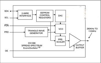
Antenk offers a variety of high quality and competitively priced 1.27mm pitch single,dual, three and quad row pin (male) headers used in many board-to-board PCB connections, fitting small-sized, densely-packed devices.
This low-profile component is made from high-temperature thermoplastic and is offered with several means of connections and mounting styles such as through-hole (THM) or surface mount (SMT) and can be in vertical (straight), elevated or at a right angle configuration/orientation dissipating current of about 1.0 A or less.
Small equipment and devices can highly benefit from the small but robust stature of the 1.27mm pitch Pin Header as its material is tested for high-vibration and shock requirements of the automotive, industrial, and consumer electronics industries. This 1.27mm pitch pin header is widely used in diverse applications such as:
Medical Diagnostic and Monitoring equipment
Communications: Telecoms and Datacoms
Industrial and Automotive Control and Test
Retail and Point-Of-Sale equipment
Mil/Aero and Home Security
Solar applications
Weighing systems
Vehicle infotainment
Computer peripherals
Telecommunications
Heart monitors
Mount Type:
Through-hole vs Surface Mount
1.27mm pitch pin (male) headers are offered in either Surface-mount or Through-hole mount termination. At one side of this pin header is a series of pins which can either be mounted and soldered directly onto the surface of the PCB (SMT) or placed into drilled holes on the PCB (THM).
Through-Hole (Poke-In)
Best used for high-reliability products that require stronger connections between layers.
Aerospace and military products are most likely to require this type of mounting as these products experience extreme accelerations, collisions, or high temperatures.
Useful in test and prototyping applications that sometimes require manual adjustments and replacements.
1.27mm vertical single row header, 1.27mm vertical dual row header, 1.27mm Elevated single row pin header, 1.27mm Elevated dual row pin Header, 1.27mm Right-angle single row header and 1.27mm Right-angle dual row header are some
examples of Antenk products with through-hole mount type.
Surface-Mount
The most common electronic hardware requirements are SMT.
Essential in PCB design and manufacturing, having improved the quality and performance of PCBs overall.
Cost of processing and handling is reduced.
SMT components can be mounted on both side of the board.
Ability to fit a high number of small components on a PCB has allowed for much denser, higher performing, and smaller PCBs.
1.27mm Right-angle Dual Row pin header, 1.27mm SMT Single row pin header, 1.27mm SMT Dual row pin header and 1.27mm Elevated Dual Row Pin Header are Antenk`s SMT pin headers.
Soldering Temperature for 1.27mm Pitch Pin Headers
Soldering SMT pin connectors can be done at a maximum peak temperature of 260°C for maximum 60 seconds.
Vertical (Straight) and Right-Angle
1.27mm pitch headers may be further classified into pin orientation as well, such as vertical or straight Male Header or right-angle male header.
Vertical or Straight Pin (Male) Header Orientation
One side of the series of pins is connected to PCB board in which the pins can be at a right-angle to the PCB surface (usually called "straight" or [vertical") or..
Right-Angle Pin (Male) Header Orientation
Parallel to the board's surface (referred to as "right-angle" pins).
Each of these pin-types have different applications that fit with their specific configuration.
Pcb Connector Stacking
Elevated Pin Header Orientation
Elevated pins aka Stacked Pins or Mezzanine are simply stacked pin headers providing an exact distance requirement between PCBs that optimizes electrical reliability and performance between PCB boards.
Profile Above PCB
This type of configuration is the most common way of connecting board-to-board by a connector. First, the stacking height is calculated from one board to another and measured from the printed circuit board face to its highest insulator point above the PCB.
Single, Dual or Multiple Number of Rows
For a 1.27mm straight or vertical Male Pin Header, the standard number of rows that Scondar offers ranges from 1 to 2 rows. However, customization can be available if 3, 4 or n number of rows is needed by the customer. Also, the number of contacts for the single row is about 2-50 pins while for dual row, the number contacts may vary from 4-100 pins.
Pin Material
The pins of the connector have been designed with copper alloy. With customer`s demand the pins can be made gold plated.
Breakaway design
The pin headers are also equipped with a breakaway design making them fully compatible with their female receptacles.
Custom 1.27mm Pitch Pin Headers
Customizable 1.27 mm pitch pin headers are also available, making your manufacturing process way faster as the pins are already inserted in the headers, insulator height is made at the right size and the accurate pin length you require is followed.
Parts are made using semi-automated manufacturing processes that ensure both precision and delicacy in handling the headers before packaging on tape and reel.
Tape and Reel Packaging for SMT Components
Antenk's SMT headers are offered with customizable mating pin lengths, in which each series has multiple numbers of circuits, summing up to a thousand individual part number combinations per connector series.
The tape and reel carrier strip ensures that the headers are packaged within accurately sized cavities for its height, width and depth, securing the headers from the environment and maintaining consistent position during transportation.
Antenk also offers a range of custom Tape and reel carrier strip packaging cavities.