Big cattle trick: teach you to improve your own RF sampling
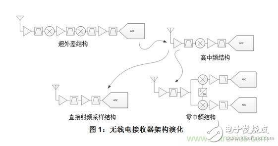
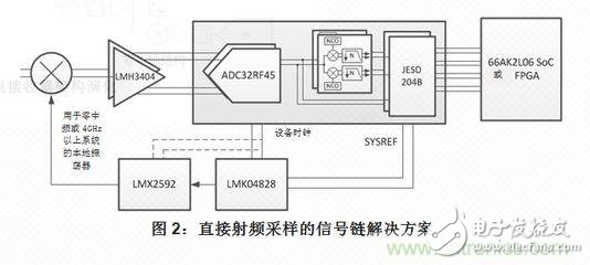
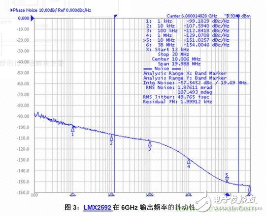
Over the past decade, radio-receiving architectures such as wireless communications and military systems have grown tremendously, thanks in large part to the innovation of high-speed analog-to-digital converters (ADCs). Ten years ago, most radios were built on a relatively basic superheterodyne structure with multiple downconversion stages. At the time, we witnessed a single downconversion change in the high IF (intermediate frequency) architecture. This is due to the significant improvement in ADC bandwidth, sampling rate and performance, which enables signal sampling in the second or third Nyquist zone. The ADS62P45 ADC is a typical example of this change. Now, ADC technology has been further improved and enhanced to eliminate the last downconversion stage in the radio, supporting direct radio frequency (RF) sampling receivers. See Figure 1. ADCs that can be used in direct RF sampling radio architectures have been on the market for many years, such as Texas Instruments' ADC12J4000. However, the ADC32RF45 is the first ADC to achieve direct RF sampling, and direct RF sampling rivals the dynamic range of superheterodyne and high IF structures. In a zero-IF architecture (zero-IF architecture is the preferred architecture for extreme broadband systems), the ADC32RF45 is the first to apply a 2GHz complex signal bandwidth on a single device. As most designers know, the performance of a data converter is only comparable to other integrated circuits (ICs) in the system. Direct RF sampling receivers or wideband zero-IF receivers can be implemented or destroyed using the appropriate equipment. Figure 2 shows some of the devices that make up the signal chain. Please take a closer look at the legend, and we'll take a closer look at some of these devices. Five components of RF sampling receiver or wideband digital converter If you just look at the data table simply, it is more difficult to select the matching devices. The relevant background (including the ADC) of the five components in Figure 2 will be presented here to present a complete, simplified and/or improved RF sampling receiver or wideband zero intermediate frequency receiver. This solution can be used in wireless infrastructure, military radar, electronic warfare or broadband communications test equipment systems. Data conversion The ADC32RF45 is the core and soul of the RF sampling receiver. It has a noise floor of -155dBFS/Hz, allowing the signal to be directly sampled at an RF frequency of 4GHz; however, it requires a high quality sampling clock to avoid the dynamic range degradation achieved by high IF structures. For signals above 4 GHz, the ADC32RF45 can be used in a wideband high IF structure or a zero IF structure with the aid of an RF synthesizer. The high sampling rate, combined with two channels in a single package, means you can use a zero IF receiver with a minimum 2 GHz signal bandwidth and minimize I/Q mismatch between ADC channels, but this requires a driver amplifier Help, the driver amplifier also needs to be very small and highly matched. The ADC32RF45 includes four integrated digital downconverters (DDCs), two per channel, for shunting the processing of logic devices. The DDC can mix the desired signal to the I/Q baseband through up to three digitally controlled oscillators per channel for observation or carrier frequency hopping applications. Next, the decimation filter reduces the data rate for direct RF sampling with the benefit of high ADC sampling rates while reducing the requirements for signal processing and ADC interface. The extracted signal is then sent to a field programmable gate array (FPGA) or digital signal processor (DSP) for additional baseband processing. Signal amplification and single-ended to differential conversion The amplifier drives the direct RF sampling structure and the ADC in the wideband zero-IF architecture. The LMH3404's dual and fully differential amplifiers operate well from DC to 2 GHz and work well with RF sampling ADCs, thanks to the 7 GHz bandwidth of the LMH3404. The purpose of the LMH3404 is to replace the transformer (balance-unbalance converter) to perform single-ended to differential signal conversion for the ADC while providing 18dB of gain. Compared with transformers, the advantage is that it can be reduced to DC at all times, which is required for broadband zero-IF systems. When paired with the ADC32RF45, the LMH3404 can be used to build small, high-performance 2GHz bandwidth zero-IF receivers for broadband communications and testing. Dual channel amplifiers have excellent channel-to-channel gain and phase matching performance, limiting the amount of digital mismatch correction required by the system. Timekeeping In RF sampling radios, the quality of the sampling clock has a strong influence on the signal-to-noise ratio (SNR) generated by the system. The LMK04828 is a JESD204B-compliant ultra-low noise clock jitter cleaner that generates clocks with less than 100fs of jitter and RF sampling capability, while offering a range of shrinking or simplified system features. Supporting up to seven JESD204B devices, the LMK04828 can clock multiple ADC32RF45 ADCs, digital-to-analog converters (DACs), FPGAs or DSPs. The LMK04828 can also generate a system reference (SYSREF) signal for deterministic latency in the JESD204B system, while digital and analog delays can help meet the critical timing requirements of each JESD204B device. For systems with high quality clocks, the LMK04828 can be used as a clock distribution device while still having SYSREF generation and delay. For all ADC32RF45 based systems, I recommend the LMK04828. Radio frequency synthesis Another option for high performance timing (especially for direct RF sampling structures) is the use of the LMX2592 RF synthesizer combined with the LMK04828. The LMX2592's high output swing and low phase noise allow it to achieve an integrated bandwidth of 12kHz-20MHz with less than 50fs root mean square (RMS) jitter, enabling multi-decibel improvement in signal-to-noise ratio at high RF frequencies, as shown in Figure 3. Shown. The LMK04828 acts as the reference clock for the LMX2592 and also generates a SYSREF signal for the deterministic delay of the JESD204B subclass 1. For systems with carrier frequencies above 4 GHz (C-band or X-band), the LMX2592 can act as a local oscillator (LO), generating signals up to 9.8 GHz and mixing the desired signals to a relatively high (up to 4 GHz) IF. The ADC32RF45 can directly sample IF signals with an IF signal bandwidth of up to 1 GHz for creating wideband, high frequency, high IF structures. In addition, the LMX2592 can be used as a local oscillator in a zero-IF architecture with up to 2GHz signal bandwidth with the ADC32RF45. Digital signal processing The ADC32RF45 is typically connected to the FPGA; however, the ADC32RF45's JESD204B digital output can be directly connected to the 66AK2L06 multi-core digital signal processor (DSP) and ARM® System-on-Chip (SoC) when using the ADC's DDC function. The ADC32RF45 is directly connected to the SoC to reduce system size, weight and power (SWaP) by removing the connected FPGA. The 66AK2L06 includes a programmable digital front end (DFE) with DDC and digital filtering that extends the processing capabilities of the ADC32RF45 to enable additional sub-band or filtering of multi-carrier RF systems. In addition, the DFE includes an automatic gain control (AGC) feature to protect the ADC32RF45 while maintaining optimal ADC performance. The KeyStone II Device DFE User Guide provides more insight into the capabilities of the ADC32RF45 and the allowable lines and rates of the JESD204B. The 66AK2L06 SoC integrates the Fast Fourier Transform Coprocessor (FFTC) to accelerate complex FFT/iFFT operations at 10-15x, making it ideal for low-latency applications. in conclusion The ADC32RF45 allows designers to eliminate the need for dynamic range trade-offs when architecting direct RF sampling radios. The Texas Instruments best signal chain components mentioned in this article, paired with the ADC32RF45, will maximize system performance: The LMH3404 acts as a DC to 2GHz ADC exciter, replacing a single-ended to differential conversion transformer (balance-to-balance converter) with DC-coupled capability and 18dB gain. · The LMK04828 generates or distributes the high performance clock required for RF sampling. The LMX2592 offers a higher performance timing option that acts as a local oscillator synthesizer in systems with carrier frequencies exceeding 4 GHz (C-band or X-band). · Connect the JESD204B output to the 66AK2L06 DSP to reduce size, weight and power (SWaP). Pcb Pluggable Terminal Block Connector ,Pluggable Terminal Block,Contact Pluggable Terminal Blocks ,Pluggable Screw Terminal Cixi Xinke Electronic Technology Co., Ltd. , https://www.cxxinke.com