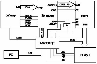
Implementation of Vehicle Low-end Image Data Acquisition Compression Storage and Transmission System
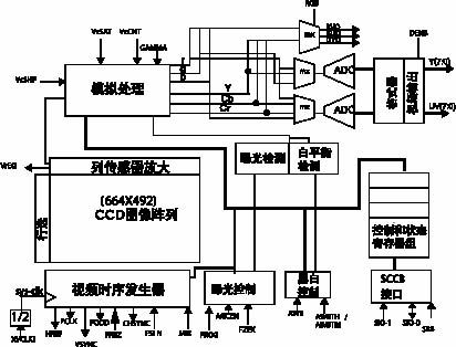
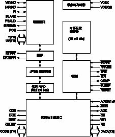
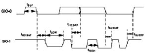
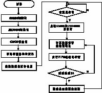
Overview This article refers to the address: http:// In some situations where unattended automatic monitoring is required, conventional image monitoring systems have some unavoidable drawbacks, such as large equipment size, high procurement costs, sufficient power supply, and inability to repeat recording. Especially in situations where continuous image acquisition is not required, conventional image monitoring systems are often not available. According to the application requirements of the long-distance bus for the on-board personnel, a set of low-end image data acquisition, storage and transmission system based on EZ-USB was developed. The system uses OmniVision's CMOS image sensor OV7620 as the acquisition chip, Zoran's ZR36060 as the data compression chip, Cypress's USB interface with the USB interface AN2131QC as the total control chip and USB data transmission chip. Since the passengers getting on and off the long-distance bus is a non-continuous process, the image data storage requirements are relatively low, so the image data is saved by Hynix's NAND flash memory chip HY27UA082G1M. This not only reduces power consumption, but also enables repetitive storage. The system also includes a FIFO for image data buffering. The image data acquisition system has the advantages of high integration and fast transmission speed, can make up for the shortcomings of the conventional image monitoring system, and is expected to fill the gap in the low-end video image field (such as a portable image system). The CMOS color image sensor OV7620 integrates the CMOS optical sensing core with the peripheral support circuit. It has functions such as programmable control and video analog/digital mixed output. It can eliminate photoelectric interference such as noise and light flicker, and output clear and stable color images. Features of the OV7620 include: single-chip 1/3-inch lens, maximum 664 × 492 pixel resolution; I2C control, standard SCCB interface; windowing function, partial image output; output RGB/RawRGB/YCbCr video signal; automatic exposure control / automatic White balance / automatic gain control / automatic brightness control; image quality control, including color saturation, sharpness, gamma correction, etc. Figure 1 is the internal block diagram of the OV7620. After video image acquisition, it is converted to digital video signal output by analog-to-digital conversion circuit and control processing. The video control timing is generated by the timing generation circuit, and the external digital signal is image data Y. [7:0] and UV[7:0]. The timing signals include an image clock PCLK, a parity field signal FODD, a line sync CHSYN, a valid pixel HREF, and a field sync VSYNC. Because it uses I2C standard SCCB control, it can use SCMB bus to simulate image frame rate, exposure time, gain control, gamma correction, etc. It can also preset image resolution, acquisition area and so on. The JPEG codec chip ZR36060 is designed for video capture and editing applications. It can easily realize real-time compression and decompression of video signals. The internal block diagram is shown in Figure 2. When compressing, the ZR36060 accepts the YUV4:2:2 digital video signal and encodes it as a JPEG stream output; when decompressed, the ZR36060 accepts the JPEG stream and decodes it into a YUV4:2:2 digital video signal output. ZR36060 has the following features: video compression and expansion, up to 25 ~ 30 frames / sec compression for pixel blocks and CCIR video signals; flexible data interface, supports three YUV video interface modes, namely 8-bit main mode, 16 Bit slave mode and 8-bit slave mode; provide synchronous master mode and synchronous slave mode. The former is to generate all timing signals inside the chip, and the latter is to synchronize the chip itself to an external video source; 3 different The bit rate control mode is used for compression of still and motion video; it can be seamlessly connected to many popular video decoders. Since the amount of data of the video image file is very large, the size of an uncompressed 8-level gray-scale black-and-white video image is 664 × 492 = 327 KB. If you don't compress the image, it will take up a lot of space in the flash memory. Therefore, the characteristics of the ZR36060 and the features that can be easily set are adopted, and the chip is used in the video capture device. The AN2131QC is a USB 1.1 protocol developed by Cypress, which makes it easy to develop USB peripherals. AN2131QC has all the features of 51 single-chip microcomputer, and the speed is faster, you can use the general instruction set of 51 single-chip microcomputer. The system design using the EZ-USB chip does not need to consider the number of endpoints, buffer size and transmission speed. Each chip is embedded with an EZ-USB core, which can handle most USB transactions, greatly simplifying the program code and speeding up the development process. As shown in FIG. 3, the entire image data system is composed of several parts: acquisition, compression, storage, and transmission. The setting of OV7620 is through the image-based digital camera serial bus SCCB. In the AN2131 MCU, the control signal cannot be directly generated. Therefore, the two pins of AN2131QC must be used for simulation. Figure 4 shows the timing of read and write transmission. In order to save space, the output mode of the OV7620 is set to a 16-bit video bus, but only the gray image data of [Y7:0], the synchronization of the captured video, and the image clock are sent to the ZR36060. Image Compression The ZR36060 uses a video sync slave, 8-bit code master and 8-bit video bus mode, ie, the microcontroller sets its internal registers by the 8-bit data bus [DATA7:0] (initialization), video clock and synchronization. The OV7620 is generated, and the ZR36060 sampling sync signal is synchronized with it. The [Y7:0] video gray signal is compressed, and the compressed JPEG image is directly sent to the FIFO buffer by the [CODE7:0] output. NAND-style FLASH may have bad blocks. This requires consideration of the correspondence between physical addresses and virtual addresses. Therefore, a correspondence table is established and exists in the first few blocks of FLASH. The table is continuously updated, with the increase of bad blocks. The change also records the location where the data is saved. In this way, the image data distribution can be directly read during initialization. In order to record the data of the FIFO, a DMA-like storage method is employed. The MCU first inputs the serial signal of the command and the calculated address from the [D7:0] port, and then issues a command to enable the RE output of the FIFO and counts. When the number of pages reaches 512 words, the above input process is repeated. After the acquisition and compression chip is initialized, it enters the control phase of image data compression, and ensures that the image data is stored in the intact FLASH data block. When the delay time arrives, the block of the oldest FLASH image data is erased. To ensure that it is used the next time you save. The block diagram of the image acquisition part is shown in Figure 5. System function introduction The system is installed in the passenger station of the long-distance bus. When a person passes, the image and acquisition process starts, and the acquisition is stopped after 3s delay. At the same time, the collected data is compressed and sent to the FLASH for storage. After setting, the resolution of the image is 640 × 480, the refresh rate is 15 frames / sec, and the image of MJPG is about 15 KB per frame after compression. The image acquired each time is 15K×3×15=675KB, so that two 256M×8Bit FLASH can record image data of 700-800 person times, which can meet the needs of the vehicle image acquisition system. 2000Puffs Disposable Vape,2000Puffs Disposable Pod Pen Device,Airis Mega E-Cigarette,Airis Mega Pod Pen Device Shenzhen Uscool Technology Co., Ltd , https://www.uscoolvape.com