Power amplifier speaker protection circuit
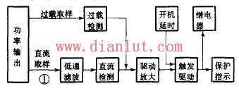
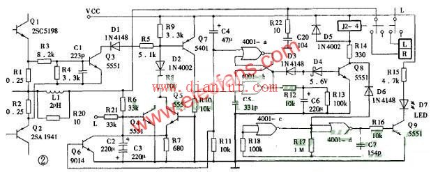
Below is the circuit diagram of the protection circuit of the amplifier speaker The block diagram of the power amplifier speaker protection circuit is shown in Figure 1. The figure contains three protection methods. (1) DC protection: when the power amplifier circuit occurs When the absolute value of the DC voltage appearing at the output end exceeds the design limit, the DC detection circuit in the protection circuit detects it and becomes a control signal. After the control signal is amplified, the control flip-flop is turned over, the protection relay is activated, and the power output circuit is disconnected to protect the speaker. At the same time, the control signal also starts to indicate the operation of the circuit, so that the protection indicator flashes an alarm. (2) Overload protection: When the output current exceeds about 1 times of the rated output current, the overload detection circuit outputs a protection control signal, and the control output circuit is disconnected to protect the speaker and the power amplifier. (3) Power-on delay-on protection: control the working state of the relay drive circuit through the power-on delay circuit, so that the relay can be turned on for 1-4 seconds after the power-on to turn on the speaker to avoid the surge current generated during the boot process. speaker. Shift the voice coil. The specific circuit is shown in Figure 2. The circuit is centered on Q4 and Q5 and constitutes a DC voltage sampling detection circuit. In the figure, Q1, Q2, etc. are right channel power output circuits (not shown in the left channel power output circuit diagram). The DC voltage sampling signal of the right channel is attenuated and isolated via R6 (left channel sampling signal via R21), filtered by C2 and C3, and sent to the complementary DC detection circuit composed of Q4, Q5 and R7 for monitoring. When the power output circuit of the right (or left) channel exhibits a positive DC offset voltage, the current is connected to ground through R6 (or R21) and Q4, and Q4 is turned on, and its collector output control level After being amplified by R8 and D2, the Q7 is amplified and sent to the RS trigger. same. When a negative dc offset voltage occurs in the power output circuit, the current passes through the ground, the BE junction of Q5, the R6 (or R21), and the midpoint of the OCL circuit. Q5 turns on and also outputs the control level. This sampling detection method is complementary. R1, R2, R3, R4, Q3, etc. constitute an overload detection circuit (the overload detection circuit of the left channel is not shown). R1 and R2 are used to sample the overload condition of the upper and lower arm power tubes of the output stage. Q3 monitors the output circuit for overload conditions. The voltage across R1 is proportional to the emitter current of power transistor Q1, which is attenuated by R3, R4, and R2 to become the forward bias of the Q1 emitter junction. Adjusting the resistance of R3 and R4 will make this voltage not turn on Q3 under the rated output state. When the power amplifier works abnormally and causes Q1 to be severely overloaded, the current flowing through R1 increases greatly. Thus, a forward bias voltage sufficient to turn Q3 on is generated, and Q3 is turned on, and the monitoring signal is outputted, and amplified by Q7 and sent to the flip-flop, so that the trigger output state is reversed, the relay is released, and the power output circuit is turned off. For example, when the instantaneous output current of the Q1 emitter reaches 10A, the voltage across R1 can reach 0.25Ω×10A=2.5V. This voltage is divided by R3, R4, and R2 and is still greater than 0.7V, which is enough to turn Q3 on. The lower arm power tube takes the voltage from both ends of R2 and divides it by R1, R3, and R4 to provide Q3 monitoring. In order for the overload protection circuit to not affect the normal use of the amplifier, C1 is added to the circuit. C1 and R3 form a filtering network to prevent Q3 from being mis-controlled by high-frequency strong signals. In addition, in order to avoid the loss of protection of Q3 damage, in some circuits, a clamp circuit composed of a resistor and a diode is added between the base of Q3 and the ground. When the voltage of the base of Q3 is too high, the voltage limiting is shunted through this circuit to protect Q3. D1 and D2 are isolated in the circuit to prevent the overload protection detection circuit and the DC protection detection circuit from affecting each other. In Figure 2, C6 is the delay capacitor, C6, R12, R13 and D4, 08 form a delay circuit. When the power is turned on, the high level of the trigger output is divided by R12 and R13 and then charged to C6. Since the voltage across C6 cannot be abrupt, its positive terminal is pulled down to ground potential at startup, and the time constant of C6's charging circuit is large, and the presence of D4 makes Q8 unable to conduct immediately. When the charging voltage of the positive terminal of C6 reaches 5.6V+0.7V≈6.3V, D4 is turned on, Q8 is also turned on, the relay is connected, and the power output circuit is turned on to achieve the purpose of power-on delay protection. The flip-flop in Figure 2 is a typical RS flip-flop consisting of a "NOR" gate in the 4001 integrated block. The C4 negative terminal is connected to the R terminal, the Q7 collector is connected to the S terminal, and the output terminal is Q and R, S. The relationship between the ends is shown in the attached table. Schedule RS Trigger Truth Table RSQ Logic Function 0 1 0 set to 0 1 0 1 set 1 1 1 unchanged 0 0 not allowed In Figure 2, C4 is the preset (initialization) capacitor of the flip-flop, that is, the R terminal is 1 when the power is turned on, so that the flip-flop outputs a high level. After the delay, the drive Q8 is turned on, and the J2-4 is connected. Turn on the speaker to work. In addition, since the power amplifier circuit cannot be completely symmetrical between the upper arm and the lower arm, the operating points of Q1 and Q2 are prone to deviation when the power is turned on, causing the output midpoint potential to deviate from 0V, and affecting the trigger through the DC detection and amplification circuit. S control terminal, the normal operation of interference delay protection. In order to avoid this phenomenon, the circuit adds Q6 between the input of the DC detection circuit and the ground. At startup, the preset voltage provided by C4 makes Q6 saturate and conduct, forcing the absolute value of the DC detection input to be much lower than 0.7V without monitoring level output. The time constant of the charging loop composed of C4 and Q6 and R11 is far greater than the time established by the operating point of the OCL circuit to ensure that the protection circuit can work reliably. In Figure 2, the protection indication circuit consisting of two NOR gates and Q9, D7, etc. in the 4001 integrated block, 4001-c, 4001-d are connected to a "non" gate, and a multi-harmonic with R17, R18, C7 Oscillator. Adjust the resistance value of the oscillator to change the oscillation frequency of the oscillator. The square wave signal output by the oscillator is isolated by R16, and then amplified by Q9 to drive D7 to flash the alarm. D6 is an isolation diode. When Q8 is saturated, the relay is connected, and the power amplifier is working normally, the feedback voltage of 4001-c is made to ground through D6, the oscillator is forced to stop, and the 4001-d output is high. Control D7 is always on. When the Q8 cut-off circuit is in the protection state, D6 is reverse-cut, avoiding the high level of the Q8 collector affecting the operation of the oscillator. An open impeller has vanes that are attached to a center hub and mounted directly onto a shaft. There is no wall surrounding the vanes which makes open impellers weaker than closed or semi-closed valves. Open impellers are generally faster and easier to clean and repair. Centrifugal pump impellers are selected with purpose and are dependent upon the application. Some are better for solids handling, others are better for high efficiency. Open Impeller,Semi Open Impeller,Open Impeller Pump,Open Type Impeller Shenyang Zhicheng Heavy Machinery Manufacturing Co., Ltd. , https://www.zhichengmachinery.com