Toshiba's new NAND chip
Toshiba Corporation announced today the introduction of a new type of embedded NAND flash memory module that integrates NAND chips manufactured using 19-nanometer second-generation process technology. This module complies with the latest e.MMC standard and is intended for use in a wide range of digital consumer products such as smart phones, tablet computers and digital video cameras. Fire Resistant Wire,Refractory Wire,Fire Resistant Insulated Wire,High Temperature Cable JIANGSU PENGSHEN HIGH TEMPERATURE WIRE CABLE CO., LTD. , https://www.pengshencable.com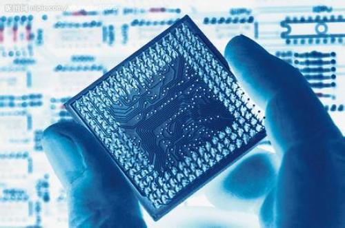
The demand for high-density NAND flash memory chips that can support high-resolution video and provide more storage space continues to grow. This is particularly evident in the field of embedded memories that contain controller functions that minimize development requirements and make integration into system designs easier. Toshiba is meeting this need by enhancing its high-density memory product line.
The company's new 32-GB embedded device integrates four 64-Gbit (equivalent to 8GB) NAND chips (made with Toshiba's 19-nanometer second-generation state-of-the-art process technology) and a dedicated control in a small 11.5 x 13 x 1.0mm package. Device. It complies with the JEDEC e.MMC Version 5.0 standard released by JEDEC in September and achieves high read and write performance through the adoption of the new HS400 high-speed interface standard.
Toshiba will use these NAND chips in a single-package embedded NAND flash family with a density of 4GB to 128GB. All devices will integrate a controller to manage the basic control functions of NAND applications.
Key Features 1. Interfaces conforming to the JEDEC e.MMC Version 5.0 standard can handle basic functions including write block management, error correction and driver software. It simplifies system development and allows manufacturers to minimize development costs and speed time-to-market for new and upgraded products.
2. Once embedded in the system, the 128GB module can record up to 2,222 hours of music, 16.6 hours of full HD video, and 38.4 hours of standard definition video at 128Kbps.
3. The new product adopts a NAND flash memory chip manufactured using a 19-nm second-generation advanced process technology.
4. The new product is available in a small 11.5 x 13mm FBGA package and has a signal layout that conforms to the JEDEC e.MMC version 5.0 standard.